
I love 3D printing as it enables me to create custom enclosures for all kind of projects. The NXP LPC-Link2 probe is great, but it lacks a protective enclosure. So I decided to create a custom enclosure. And as 3D filaments are available in different colors, I experimented with red and black and custom painting:

lpc-link2 enclosure
The NXP LPC-Link2 board comes with a 10 cm 10-pin SWD cable in a box:

LPC-Link2 OM13054 Package
As it comes without enclosure, debugging is ‘bare board’ only:

Debugging with the LPC-Link2 Debug Probe
To be able to carry the LPC-Link2 and to protect it with a nice enclosure, I have designed in several iterations a 3D printable design. It took me several iterations to get to something like this:

red with black
The 3D files have been designed with the free Autodesk 123D Software and the design is available on Thingiverse:
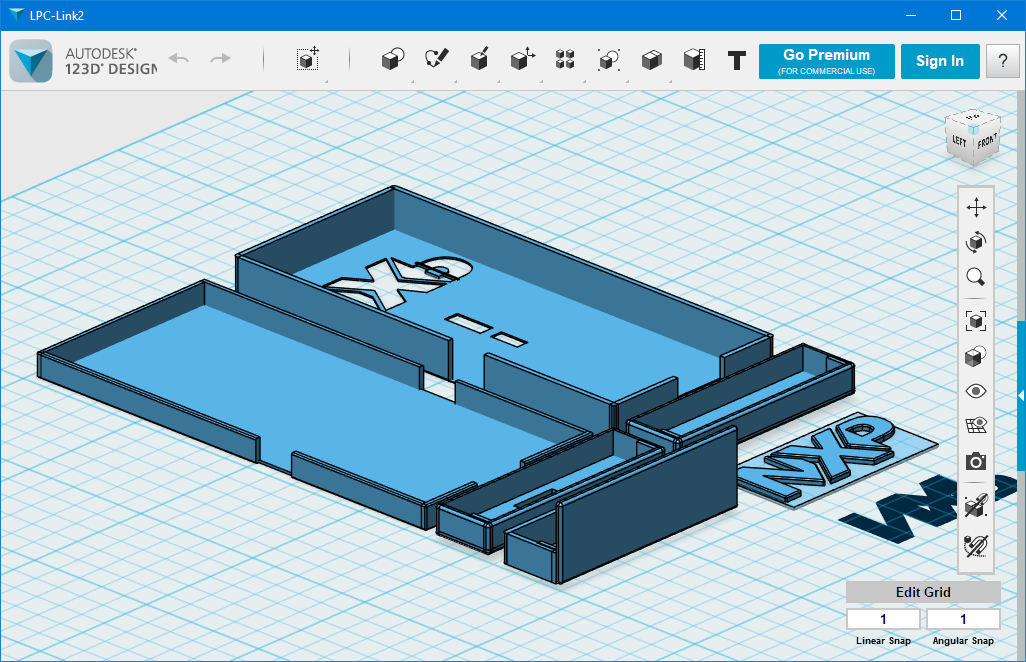
LPC-Link2 in 123D Design
Below it the bottom enclosure part:

Bottom Enclosure part
I created different NXP logo inlets. The painted one is using a white PLA filament:
NXP Logo Inlet
The hardest part is to press the small filler for the ‘P’ letter into the inlet. The inlet needs a bit glue to keep it in place:

inlet with glue

glued inlet
It does not need and nuts or bolts, and the parts easily slide together. Depending on your printer tolerances, no glueing is required. A moving slider in the middle is used to store the SWD cable:

Slider to hold SWD Cable
Here two different color variants:

Two enclosure variants
I have not decided which inlet I finally want to use, here a version with no painting:

combination of red and black
Printing the enclosure for one LPC-Link2 takes around one hour on a Ultimaker-2 (0.2mm layer height, 20% fill density) and 11g of PLA.
Happy Printing:-)

The enclosure looks great! black and red seems best one to me. This is the beauty of 3D printing that we are capable of lots of customization! cheers.
LikeLike
Yes, personally I like the black & red the most too. I feel painting ABS/PLA is ok, but it looks better if printed in different colors.
LikeLike
Pingback: MCUXpresso IDE V10.1.0 with i.MX RT1052 Crossover Processor | MCU on Eclipse
Pingback: Debugging the Teensy 3.6 with Eclipse MCUXpresso IDE and CMSIS-DAP LPC-Link2 | MCU on Eclipse
Pingback: Tutorial: Catching Rogue Memory Accesses with ARM Watchpoint Comparators and Instruction Trace | MCU on Eclipse
Pingback: Tutorial: First Steps with Embedded Artists NXP i.MX RT1052 OEM Module | MCU on Eclipse
Pingback: Tutorial: Using external Debug Probes with NXP LPC845-BRK Board | MCU on Eclipse
Pingback: Internal and External Debug Options for the NXP LPC55S69-EVK Board | MCU on Eclipse
Pingback: SWO with NXP i.MX RT1064-EVK Board | MCU on Eclipse
Pingback: Seeed Studio Arch Mix NXP i.MX RT1052 Board | MCU on Eclipse
Pingback: Debug and Execute Code from FLASH on the Seeed Arch Mix NXP i.MX RT1052 Board | MCU on Eclipse
Pingback: Enable Default FreeRTOS Debugging for LinkServer Debug Connections | MCU on Eclipse
Pingback: New MCU-Link Debug Probe from NXP | MCU on Eclipse
Pingback: Debug Firmware Switching for the LPC4322 | MCU on Eclipse
Pingback: New “MCU-Link Pro”: Debug Probe with Energy Measurement | MCU on Eclipse