One great thing with that new NXP LPC845-BRK board is that it is possible to use it with any standard SWD/JTAG debugger, as it has the 10pin debug header present on the board. It is not populated by default, because the LPC845-BRK includes a CMSIS-DAP debug probe already. But if I want to use a SEGGER J-Link, a P&E Multilink or the NXP LPCLink2, this is certainly something to consider:

Debugging LPC845-BRK with LPC-Link2
To enable debugging the board with an external debug probe. I have to populate JP1 (Jumper) and CN3 (standard 10pin SWD header):

JP1 and CN3 on NXP LPC845-BRK Board
The jumper header and jumper is part of the kit content (see Unboxing the NXP LPC845-BRK Board), the SWD/JTAG header can be ordered from the usual stores, e.g. Samtec FTSH-105-01-L-DV-K from Digikey or from Mouser.

10pin SWD Debug Header

CN3 on LPC845-BRK (Source: NXP)
On the board there is the JP2 jumper which can be used if using an external debug probe:

JP2 on LPC845-BRK

E_RST on LPC845-BRK schematics (Source: NXP)
JP2 is used to keep LPC11U325 CMSIS-DAP probe in Reset. If the debug probe is not used or under debug control, it seems to tristate the debug lines and does not affect the SWD debug lines. So using that jumper is not really needed unless I want to really silence the LPC11U35.
UPDATE: during this article I did not had the need somehow to have JP2 installed. But I really recommend having it installed with a jumper if using an external debug probe. Otherwise it could happen that you are not able to debug it.

J2 installed on LPC845-BRK
The first step is to remove the solder which is on the pads for the SWD header as the solder mask for the board did not keep them out.
I’m using standard de-solder wick or braided copper for this:

De-Solder-Wick
Removing the solder from the pads:

removing solder from pads
I remove the solder because I want the header to be on the pads, not floating on the solder. Below the board with the solder removed:

LPC845-BRK with SWD Header
Then put the header on the pads. I recommend to solder first one pad and with this align carefully the other pins. Then solder all pads.

Added SWD Header
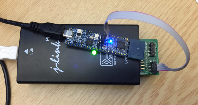
With this I was able to debug the board with a SEGGER J-Link, P&E Multilink Universal or the NXP LPC-Link2 (below with a 3D printed custom enclosure):
Debugging LPC845-BRK with LPC-Link2 (Power provided by LPC-Link2)
Debugging LPC845-BRK with J-Link

Debugging LPC845-BRK with PEMicro

Debugging LPC845-BRK with MCUXpresso IDE 10.3.0
Summary
The LPC845-BRK has an onboard CMSIS-DAP debug probe, so an external debug probe is not needed. But I love to have direct access to the CPU and freedom of choice for the debug probe I want to use. So adding that SWD gives me all the flexibility I need.
List of articles about the LPC845-BRK board:
- Unboxing the NXP LPC845-BRK Board
- Tutorial: Using external Debug Probes with NXP LPC845-BRK Board
- Tutorial: Transforming the NXP LPC845-BRK into a CMSIS-DAP Debug Probe
- Tutorial: Blinky with the NXP LPC845-BRK Board
Happy Soldering 🙂
Links
- Unboxing the NXP LPC845-BRK Board
- LPC845-BRK Board web page: https://www.nxp.com/LPC845Breakout
- User Guide for LPC845-BRK Board: https://www.nxp.com/docs/en/user-guide/UM11181.pdf
- NXP LPC845 web page: https://www.nxp.com/products/processors-and-microcontrollers/arm-based-processors-and-mcus/lpc-cortex-m-mcus/lpc800-series-cortex-m0-plus-mcus/low-cost-microcontrollers-mcus-based-on-arm-cortex-m0-plus-cores:LPC84X?
- MCUXpresso SDK: http://mcuxpresso.nxp.com/
- MCUXpresso IDE: New NXP MCUXpresso IDE V10.3.0 Release
- List of community projects: https://community.nxp.com/community/lpc/blog/2019/02/02/lpc845-brk-board-projects

Pingback: Tutorial: Transforming the NXP LPC845-BRK into a CMSIS-DAP Debug Probe | MCU on Eclipse
Pingback: Unboxing the NXP LPC845-BRK Board | MCU on Eclipse
Pingback: Tutorial: Blinky with the NXP LPC845-BRK Board | MCU on Eclipse
Hi, JP1 is not needed here. It’s for current measurement only. And CN3 isn’t necessary as well. The SWD pins PIO02 and PIO03 are accessible on pin 36 + 37 of the board.
LikeLike
Yes, JP1 was wrongly labeled in the original user manual, so it is indeed optional. Good hint about pins 36+37, but I find it easier to use it with a standard debug header.
LikeLike
Pingback: Black Magic Open Source Debug Probe for ARM with Eclipse and GDB | MCU on Eclipse
Hello friends, i´m looking a tutorial of as conecting the RS232(BLUETHOOT) and ESP8266(WIFI), so thanks for your help….
LikeLiked by 1 person
RS-232 is not Bluetooth? But have a look at https://mcuoneclipse.com/2014/11/30/tutorial-web-server-with-the-esp8266-wifi-module/
LikeLike