The NXP LPC845-BRK board is a tiny an inexpensive (sub $6) breakout board. The board includes a CMSIS-DAP (LPC11U35) on-board debug probe which can be used as a debug probe to debug any NXP LPC, Kinetis or i.MX RT device 🙂

LPC845-BRK used to debug a Sumo Battle Robot
The LPC845-BRK board features the JP1 cut-trace jumper. The intend of that jumper is to measure the current of the target CPU. But actually this jumper can be used to turn the board into a (undocumented?) general purpose CMSIS-DAP debug probe. I have tested it with the MCUXpresso IDE and have been able to debug Kinetis, LPC and i.MX RT boards that way. So with $6 I have not only a cool and tiny development board, with the addition of a SWD header, a SWD cable and a jumper I have cool and tiny debug probe :-).
Here are the steps to turn the LPC845-BRK into a general purpose debug probe:
- Solder a SWD header to the board, see Tutorial: Using external Debug Probes with NXP LPC845-BRK Board

Added SWD Header
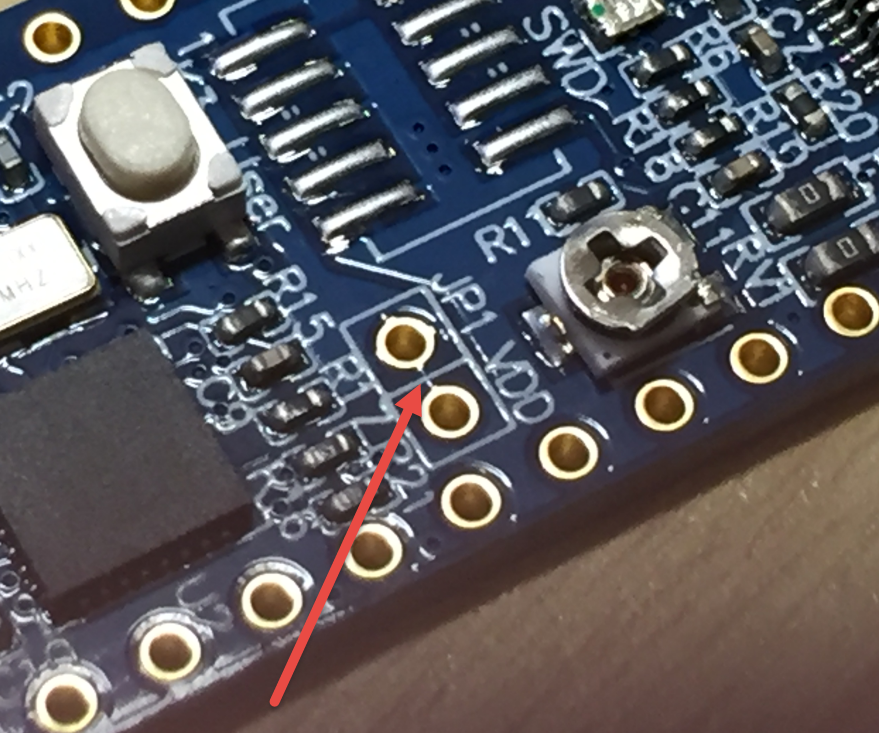
- Locate the JP1 on the board. There is a tiny PCB trace between the pads. Use a knife to cut that trace.

JP1 trace to cut
- I recommend to solder a jumper on JP1. That way I can use the board both as development board (JP1 installed) and as a CMSIS-DAP Debug probe (JP1 removed)

Installed Jumper JP1 on NXP LPC845-BRK
- Use a standard 10pin SWD cable to connect to the target

SWD Cable Connected
- The MCUXpresso IDE automatically detects the LPC11U3x CMSIS-DAP debug probe:

LPC11U3x in MCUXpresso IDE
- With this I can debug any ARM Cortex supported by the MCUXpresso IDE or any other CMSIS-DAP debugger:

Debugging i.MX RT1064 with LPC845-BRK Board

i.MXRT1064 board with LPC845-BRK as debug probe


Summary
With very small changes I can turn a normal $6 NXP LPC845-BRK board into a CMSIS-DAP debug probe to debug external Kinetis, LPC or i.MX boards. I’m able to do this with the NXP MCUXpresso IDE, but that should work with other IDE’s too. All what I need is a knife, a jumper and 2pin header with a SWD cable and connector.
Does this make my P&E, Segger or LPC-Link2 debug probes obsolete? Definitely not, because other probes offer different features or are faster. For example I measured a 3-5x faster Flash programming with the LPC-Link2 ($20) compared to the LPC11U35 ($6) based debug probe. Still, for that $6 it is a very decent debugging experience. For me every $ spent on debug probes is always a good investment, and having more probes at hand is definitely a plus, especially if they are inexpensive like this one :-).
List of articles about the LPC845-BRK board:
- Unboxing the NXP LPC845-BRK Board
- Tutorial: Using external Debug Probes with NXP LPC845-BRK Board
- Tutorial: Transforming the NXP LPC845-BRK into a CMSIS-DAP Debug Probe
- Tutorial: Blinky with the NXP LPC845-BRK Board
Happy Transforming 🙂
Links
- LPC845-BRK Board web page: https://www.nxp.com/LPC845Breakout
- User Guide for LPC845-BRK Board: https://www.nxp.com/docs/en/user-guide/UM11181.pdf
- NXP LPC845 web page: https://www.nxp.com/products/processors-and-microcontrollers/arm-based-processors-and-mcus/lpc-cortex-m-mcus/lpc800-series-cortex-m0-plus-mcus/low-cost-microcontrollers-mcus-based-on-arm-cortex-m0-plus-cores:LPC84X?
- MCUXpresso SDK: http://mcuxpresso.nxp.com/
- MCUXpresso IDE: New NXP MCUXpresso IDE V10.3.0 Release
- List of community projects: https://community.nxp.com/community/lpc/blog/2019/02/02/lpc845-brk-board-projects

Wow, this makes it even more appealing, for students especially. I wanted to start working with LPC controllers because they have 9-bit SPI, I will get one soon.
LikeLike
Hi David,
Yep, this is what I thought too! The board manual did not mention the possibility to use the board as a debug probe. Usually it is required to disconnect the SWD clock or data line, but in this case it was enough not to power the LPC845 :-). 9-bit SPI is interesting, I never needed it. For what do you need it?
LikeLike
I use some cheap Nokia color LCD displays for embedded projects, they are 9-bit SPI. With Kinetis MCUs you are stuck with 8-bit SPI so always bit-banging and its much slower I hear. would love to see improved speeds. Although I have never actually tried doing DMA for the data transfer like you did with the WS2812B. Hardware SPI sounds easier.
LikeLike
DMA is a very complicated beast. It took me about a week to get it running for the WS2812B. The issue is that it is nearly impossible to debug it, all what you can do is maybe to toggle some pins. Documentation is lacking information, or the provided examples are not well documented. It is not impossible, but I have to say compared to any other MCU peripherals the DMA one was the hardest for me. And it is different from one MCU to another too.
LikeLike
Pingback: Tutorial: Using external Debug Probes with NXP LPC845-BRK Board | MCU on Eclipse
Pingback: Unboxing the NXP LPC845-BRK Board | MCU on Eclipse
Pingback: Tutorial: Blinky with the NXP LPC845-BRK Board | MCU on Eclipse
Hi Erich,
do you have any idea to put a j-link firmware into CMSIS-DAP of LPC845-BRK.
Cai.
LikeLike
Hi Cai,
In my understanding this is not possible. It is only possible to do this with a LPC-Link2 (see https://www.segger.com/products/debug-probes/j-link/models/other-j-links/lpcxpresso-on-board/) but not with a LPC11U35 based circuit.
LikeLike