The Teensy boards are great, but as they are they are not really useful for real development, as they lack proper SWD debugging. In “Modifying the Teensy 3.5 and 3.6 for ARM SWD Debugging” I have found a way to get SWD debugging working, at that time with Kinetis Design Studio and the Segger J-Link. This article is about how debug the Teensy with free MCUXpresso IDE and the $20 NXP LPC-Link2 debug probe:
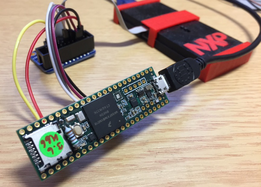
Teensy 3.6 with NXP LPC-Link2
To debug the Teensy 3.5 or 3.6, you need:
- MCUXpresso IDE (I’m using v10.1.0)
- The NXP MCUXpresso SDK for the K66FX1M0
- Modified Teensy (see Modifying the Teensy 3.5 and 3.6 for ARM SWD Debugging for instructions)
- The LPC-Link2 Debug probe (http://www.nxp.com/products/microcontrollers-and-processors/arm-processors/lpc-cortex-m-mcus/lpc1100-cortex-m0-plus-m0/lpc-link2:OM13054)
- A SWD/JTAG adapter, e.g. from Adafruit (https://www.adafruit.com/product/2094)
- Mini and Micro USB Cables
- Headers to be soldered on the backside of the Teensy
- Jumper cables
First, modify the Teensy (Some suggest it should be possible to pull down the reset line, but I had to completely remove the KL02Z from the Teensy) and solder the headers on the back side of the Teensy.
Then use the Jumper wires to connect the Teensy with the SWD/JTAG adapter:
- 3.3V to pin 1 (VTref)
- Reset to pin 15 (RESET)
- G to pin 4 (GND)
- DE to pin 6 (GND)
- DD to pin 7 (TMS)
- DC to pin 9 (TCK)
The following pictures illustrate the connection:
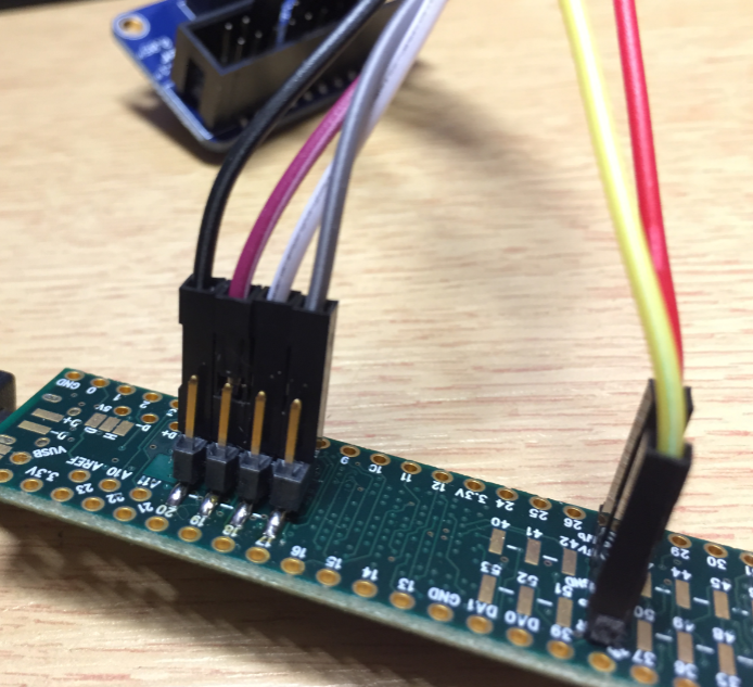
Connections on the Teensy
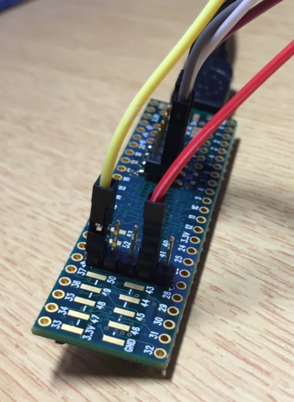
Teensy 3.6 Connection Wires
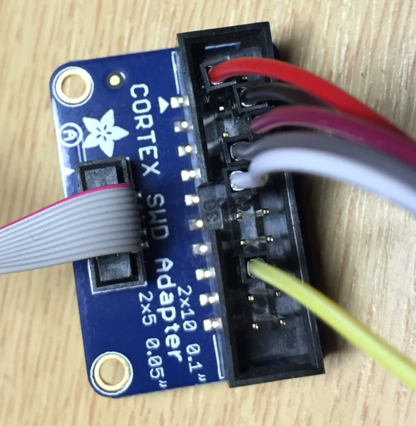
Connections on Cortex SWD Adapter
Power the Teensy board and connect the LPC-Link2 to the SWD debug adapter. I’m using a custom 3D printed enclosure for my LPC-Link2:
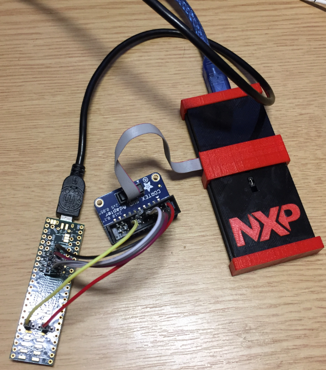
LPC-Link2 with Teensy
Inside the MCUXpresso IDE, create a project for the MK66FX1M0VMD:
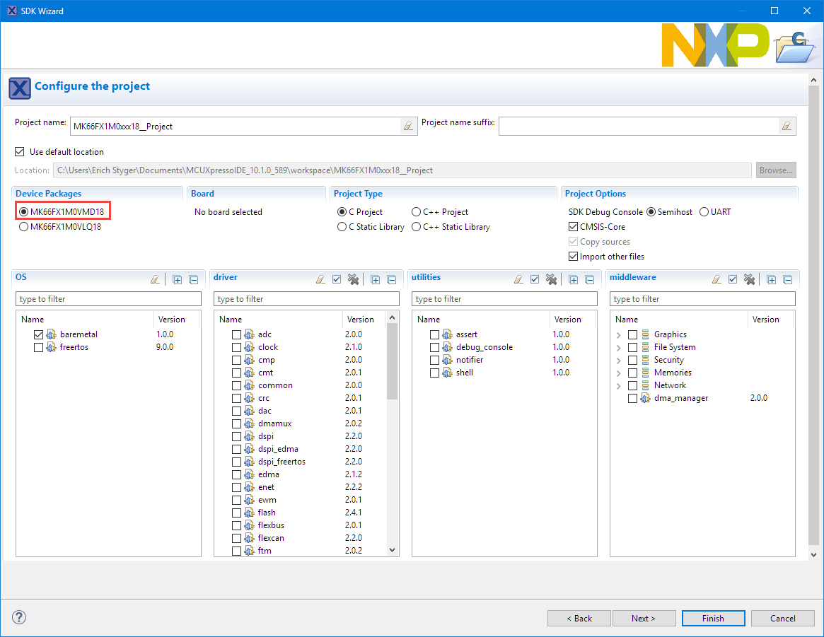
MK60FX1M0VMD18
Build it, then debug. This works fine with the MCUXpresso IDE 10.1.0:
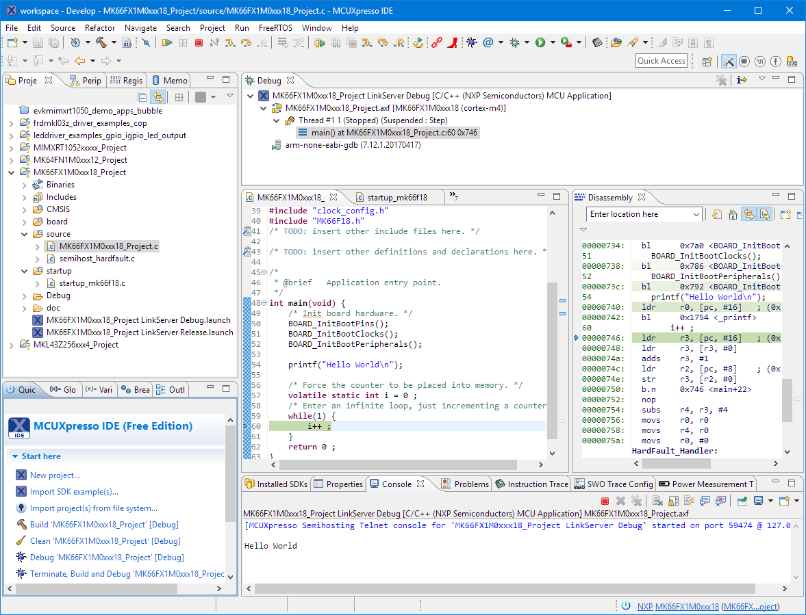
Debugging Teensy 3.6 with MCUXpresso IDE and LPC-Link2
Summary
It *is* possible to debug the Teensy 3.5/3.6, but it requires a hardware modification. Any SWD/JTAG debug probe can be used for this, including the NXP LPC-Link2 CMSIS-DAP probe.
Happy Teensing 🙂
Links
- Modifying the Teensy 3.5 and 3.6 for ARM SWD Debugging
- NXP LPC-Link2: http://www.nxp.com/products/microcontrollers-and-processors/arm-processors/lpc-cortex-m-mcus/lpc1100-cortex-m0-plus-m0/lpc-link2:OM13054
- MCUXpresso IDE: http://www.nxp.com/mcuxpresso/ide/download
- SWD debugging the Teensy v3.1: https://mcuoneclipse.com/2014/08/09/hacking-the-teensy-v3-1-for-swd-debugging/
- MCUXpressso 10.1.0 IDE: Eclipse MCUXpresso IDE 10.1 with integrated MCUXpresso Configuration Tools
- Teensy v3.5: https://www.pjrc.com/store/teensy35.html
- Teensy v3.6: https://www.pjrc.com/store/teensy36.html
- Custom 3D Printed Enclosure for NXP LPC-Link2 Debug Probes
- Adafruit JTAG/SWD Adapter (https://www.adafruit.com/product/2094)

Santa Claus has the right idea !
LikeLike
Possible alternative to Teensy, the MAX32630FTHR, but not sure if these Maxim’s are SWD/JTAG debug’able by default using Eclipse/OpenOCD (instead of DAPLINK); the pins are directly available on header though:
https://www.maximintegrated.com/en/products/microcontrollers/low-power-microcontrollers.html
LikeLike
Maybe it is only me, but my experience with Maxim ARM Cortex devices has not been positive (mostly on the software and tools side). And if I only would use them with a P&E or Segger interface as I was not able to get the OpenOCD working on them. Because there are really no or inadequate alternatives to the Teensy, we decided to make our own boards: https://mcuoneclipse.com/2018/02/10/tinyk22-boards-arrived/
LikeLike
Pingback: Overview of MCUXpresso IDE v10.2.0 | MCU on Eclipse
Pingback: Open Source RISC – Eclipse with RISC-V on the SiFive HiFive1 Board | MCU on Eclipse
Pingback: Tutorial: MCUXpresso SDK with Linux, Part 2: Commandline Debugging with GDB | MCU on Eclipse