
Europe is currently facing an ‘Energy Crisis,’ and ‘Sustainability’ is a popular topic among companies. However, embedded engineers go beyond talking—they take action and make tangible changes in the world. With the increasing use of electronic devices, minimizing their energy and power consumption is crucial. Optimizing systems for deep low power or deep low energy is a challenging task. Nonetheless, as I will demonstrate in this article, it is possible to reduce energy consumption by a factor of 100 or more. This article provides a brief overview of the foundational concepts and then applies them step-by-step to an ARM Cortex microcontroller.
Outline
At the Lucerne University of Applied Sciences and Arts I’m teaching the topic of low power optimizations in a lecture and course with labs. I have been asked if I could share and publish parts of it on my blog. That way you could use it for your learning or exploring ways how to optimize a MCU application for low power.
Software and Tools
For this article, I’m using the following:
- NXP MCUXpresso IDE 11.9.1, Eclipse based.
- NXP MCU-Link Pro Debug and power measurement too.
- NXP LPC804 ARM-Cortex microcontroller.
The MCU-Link Pro is ideal because it is a CMSIS-DAP debug probe which can be programmed as a J-Link, plus it includes the NXP LPC804 ARM Cortex-M0+ MCU (15 MHz, 32 kByte FLASH, 4 KByte SRAM) onboard, which can be used for experiments and measurements. This makes the setup very simple and easy. Especially for learning low-power optimizations the MCU-Link Pro is ideal: I get a J-Link+CMSIS-DAP debug probe plus target MCU plus power/energy measurement for less than $50.
💡 The MCU-Link is great and cost effective starting point for low power optimizations and power measurements. I get a lot of value for $50. But for very deep power down modes and accurate measurement, I have to use measurement hardware and software which easily costs $1000 or more.
Of course you could use any other tool, IDE or microcontroller you have at hand: the steps can be easily applied to a different setup.
In the next section I go over the LPC804 which will be our DUT (Device under Test).
LPC804
The LPC804 is an ARM-Cortex M0+ from NXP. It is a simple MCU, and that makes it easier as a learning platform and for this tutorial.
Below is the schematic part for the LPC804 on the MCU-Link Pro:
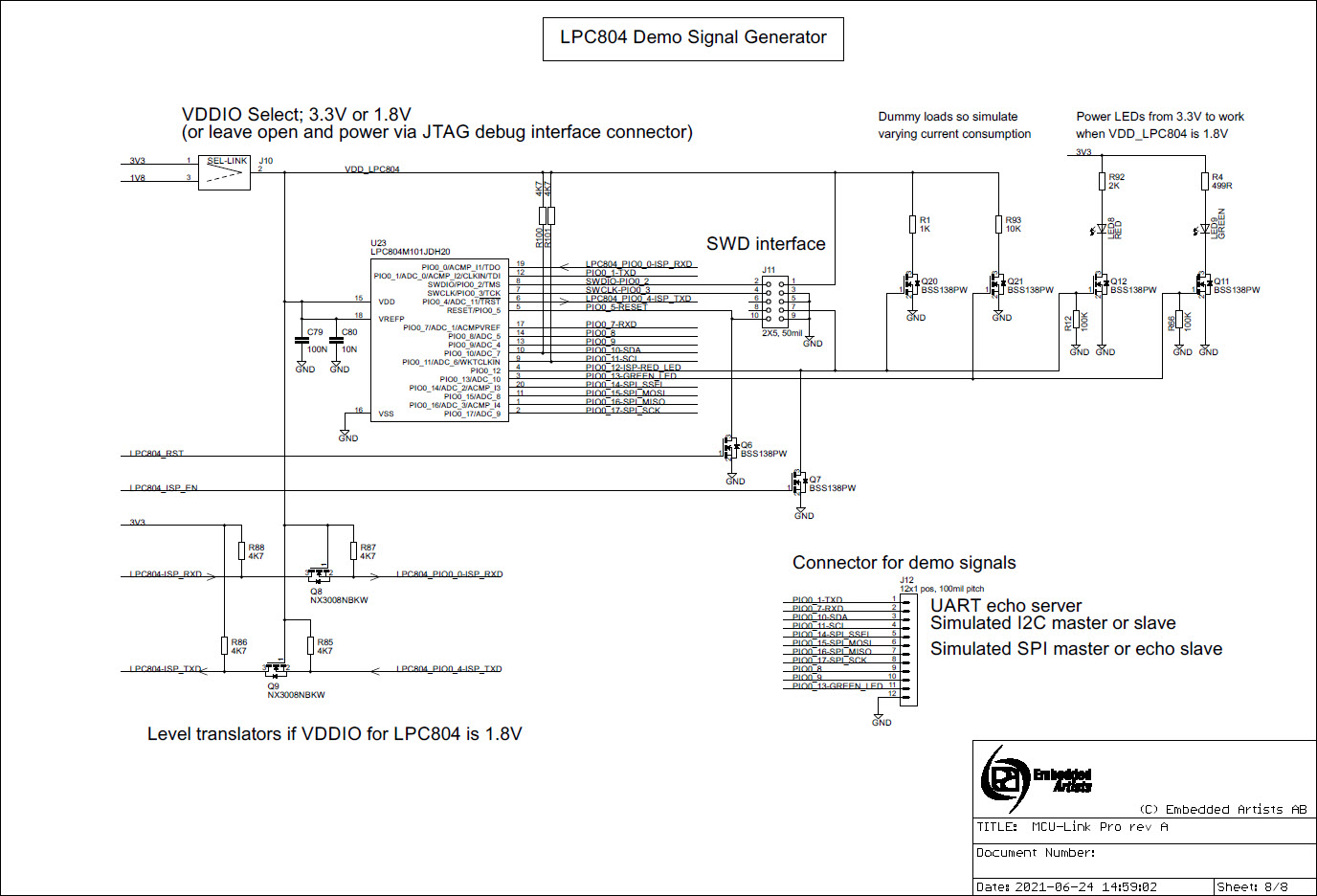
Using J10, the MCU can be powered with 3.3V or 1.8V. The green and red LED are both powered from the MCU-Link Pro 3.3V supply, and a 1K (R1, ‘red’) and 10K (R93, ‘green’) resistors are used to ‘simulate’ different loads.
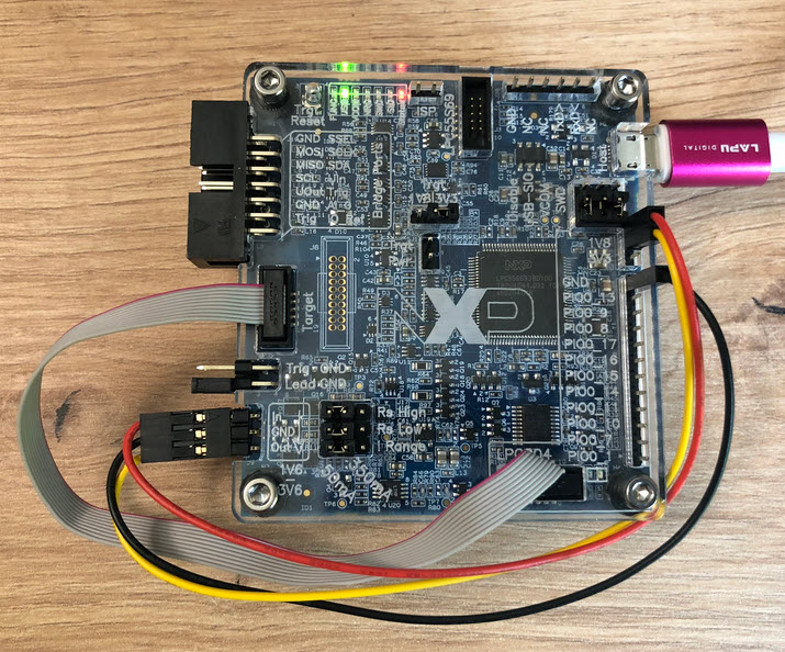
Below is how the basic wiring I’m using: the probe measurement circuit is connected to J1, and that way I can switch between 1.8V and 3.3V:
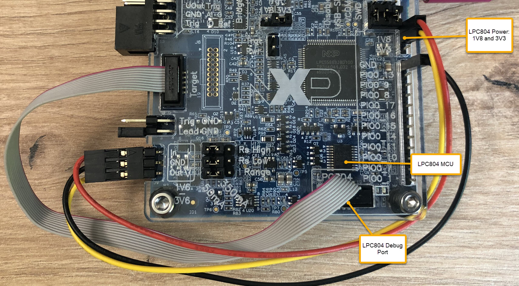
To debug the LPC804, connect the debug cable of the MCU-Link Pro as shown above to the on-board LPC804.
💡 Note that in the measurements below I run the measurements with the MCU-Link Pro without the debug process running in the background. Otherwise the measurement data will be affected by the debugger.
Next, let’s look at some of the basics behind ‘low power’ and ‘low energy’.
Theory (simplified)
I’m not going to cover the theory behind low power in details here. As a main rule: to have a low power design, then this has to be applied from the very first beginning. Means it has to be part of the hardware design *and* software design. Applying low power at the end won’t give great results. Still it is possible to reduce energy and power consumption for an existing design, although probably with limited results.
We are talking here about ‘low power’, more precisely about electrical power P which is the product of voltage and current or the green area in the following picture:
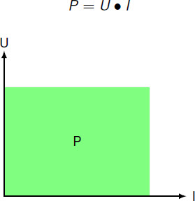
To reduce P, we can reduce U and/or I to minimize the area in above graph: the smaller the area, the smaller the power. If we can reduce the voltage and keep the current the same or smaller, we are getting better. If we can try to reduce the current needed for a given voltage. In a typical embedded design, maybe the voltage (supply voltage) could be considered constant: in that case we focus on reducing the current needed.
In the context of low power designs, especially if they using an energy storage or battery, then the electrical energy E is the main focus, which is the integral of P over time:
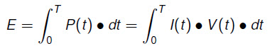
Or to visualize it: the energy is the green area built by P over time: To reduce the energy, we have to minimize the area built by P over time.
💡 Takeaway: Perform work as fast as possible (P high only for a short time), then go into sleep mode for a long time (P down to zero for a long time).
Next, we need to look at what builds up P. Considering a very simplified silicon transistor model, then the power used can be considered as the following:

Basically the total power is the power needed for switching the transistor, plus a short circuit power during the switching plus a leakage power. The first terms of the sum are dynamic and depend on the switching frequency f and the time of the short circuit. The last term of the sum is static and represent the inherent leakage of the circuit.
Applying the formula to a MCU, we can see can consider the following approaches:
- Reducing the voltage Vdd. It has quadratic impact on the first term of the sum, and a linear impact on the other. Or changing the voltage or completely cut off the supply voltage for parts of the MCU or circuit (voltage scaling or voltage gating).
- Reducing the frequency f. In terms of MCU this means reducing or changing the clock speed (gear shifting) or disable the clock for part of the MCU (clock gating).
- The Cload is basically proportional to the silicon area used. So we can consider a smaller MCU (less memory, less peripherals, or only what is needed) or consider using a MCU built in 40-nm instead of 90-nm process (although with smaller structures the static leakage increases exponentially!).
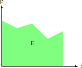
In this context, it is worth to have a look at a MCU silicon or die image, to get an idea of the area required for a given functionality. Below is a die image of an STM32F051R8T6 ARM Cortex-M0 (48 MHz, 64 KByte FLASH and 8 KByte SRAM):
We can observe that the SRAM needs more space per KByte compared to the FLASH area, and that ADC/DAC are expensive in terms of space, which turns into costs and Cload plus leakage. So the approach is to disable clocking and supply voltage of as many areas as possible, and only using a device with the needed functionality.
Notice the die size needed for the Cortex-M0 core. The M0 compared to the M3 and M4 is optimized for costs and therefore for a smaller silicon area. The M0 (and M0+) does not have a hardware integer division implemented, which otherwise would count up to 30% of extra silicon area. This means that integer divisions would have to be executed in multiple (runtime) instructions, making integer divisions much slower than using an M4 instead.
💡 Takeaway: Use the lowest possible supply voltage, try reducing the clock speed while still performing the work as fast as possible. Disable clocking and cut supply voltage in as many areas as possible. Avoid integer divisions on ARM Cortex M0. Use a device with only the needed amount of peripherals, with just enough RAM and FLASH to perform the required work.
Safety Belt and Rescue Line
Experimenting with low power modes might be dangerous: if you quickly enter a deep low power mode, then it might be impossible for the debugger to regain access to the MCU quickly enough. That’s why I always use a safety belt or rescue line in my non-production code, making sure with a delay after power-on that the debugger has enough time to regain access. Typically I call a routine like below from main() which blinks an LED to have a visual cue:
static void safetyBelt(void) {
  /* delay for safety, to be able to re-take control with the debugger */
  for(int i=0;i<10;i++) {
    LEDS_Neg(LEDS_RED);
    McuWait_Waitms(1000);
  }
  LEDS_Off(LEDS_RED);
}
This gives me time to catch the device if something is going wrong, or if I have to disable debug access for low power later in the application.
Work for MCU
The question is now: what do we want the MCU to perform? For the sake of this tutorial, I’ll keep it to this very simple steps: The MCU shall do the following work with 1 H7:
- Turn on the green LED.
- Perform multiple times a SelectionSort to simulate some workload.
- Turn off the green LED.
- Wait 1 second and continue restart with step 1.
We will measure the energy used for one full iteration.
Next, I’m going through different optimization steps.
Starting Point: Bare Metal Loop
To implement the work for the MCU, here is a simple bare-metal implementation:
safetyBelt();

int arr[] = {0, 23, 14, 12, 9};
for(;;) {
  LEDS_On(LEDS_GREEN);
  for(int i=0; i<500; i++) {
    selectionSort(arr, sizeof(arr)/sizeof(arr[0]));
  }
  LEDS_Off(LEDS_GREEN);
  McuWait_Waitms(1000); /* 1 Hz frequenzy */
}
McuWait_Waitms() is using NOP instructions based on the CPU clock frequency.
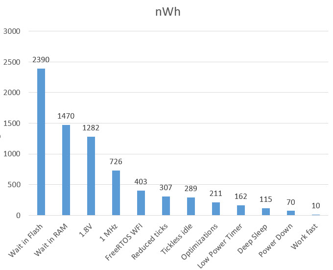
Busy Waiting in FLASH: 2390 nWh
Measuring it with as bare-metal, at 3.3V and with15 MHz, it gives the following picture with 2390 nWh for the work:
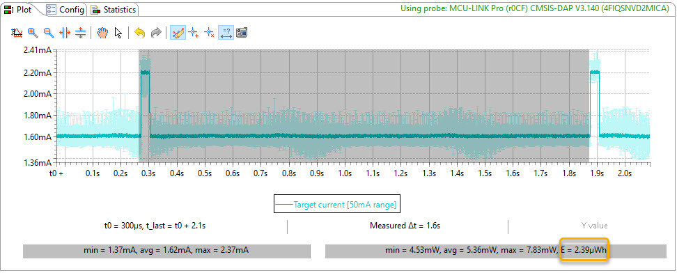
But something is strange here: The ‘blink and calculation’ needs 32 ms:
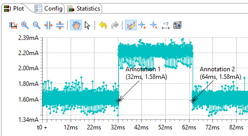
But the delay of 1000 ms takes much longer, around 1600 ms!
This means that the MCU somehow is not able to execute a NOP instruction in a single cycle? I had faced a similar issue with the LPC845 (see Doubling the performance of NXP LPC845 with improved Flash Access Time). So it means to me that running code in FLASH on the LPC804 is slower than expected.
💡 Takeaway: running from FLASH might be slow to wait cycles or slower bus access. Running code in RAM usually is faster and can speed up execution and reduce energy.
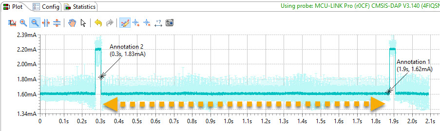
Busy Waiting in RAM: 1470 nWh
As I don’t have enough RAM on the LPC804, I had to compensate for the slower execution from FLASH with empirical adjusted number of NOPs for the wait running in FLASH:
/* McuWait */
/* LPC804 somehow is not able to execute a NOP in a single CPU cycle: */
#define McuWait_CONFIG_NOF_CYCLES_FOR_NOP_MUL   (6)
#define McuWait_CONFIG_NOF_CYCLES_FOR_NOP_DIV   (10)
Another solution is to execute the instructions for the busy waiting in RAM, and there is a simple setting for this in the McuLib:
#define McuWait_CONFIG_WAIT_IN_RAM (1) /* perform the waiting NOPs in RAM */
This is using waiting routines, running from RAM:
static uint16_t McuWait_Wait10CylesRAM[] = {
        0x46C0, /* NOP */
        0x46C0, /* NOP */
        0x46C0, /* NOP */
        0x4770, /* bx lr */
        0x46C0, /* NOP */
    };
With this, I have the expected 1000ms waiting time and 1470 nWh:
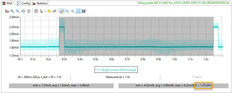
Bare Metal, 15 MHz: 1.8V => 1282 nWh
Now lets see how much going down from 3.3V to 1.8V is making a difference. That indeed helped, we are now at 1282 nWh:
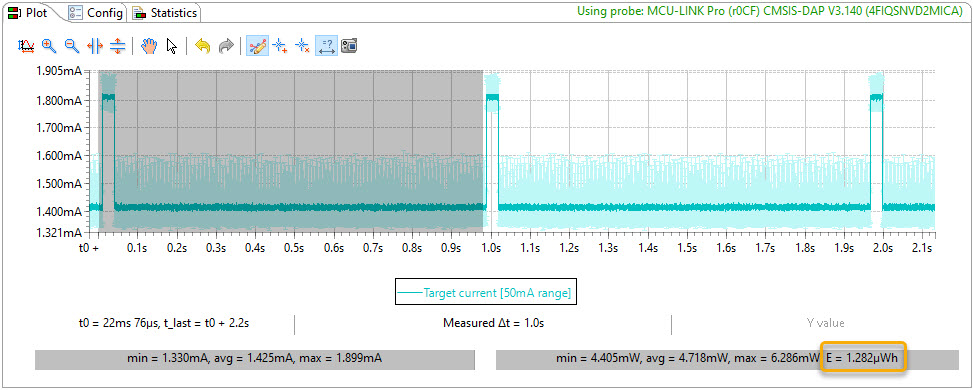
From the above formula we would have expected much more savings. But as the MCU is using internally a DC-DC converter already, the savings are not that big, but still good enough.
💡 Takeaway: reducing the voltage is a good thing, but effects might be not as big because of internal DC-DC converters already in place. Different voltage levels might require level shifters which would need to be accounted for too.
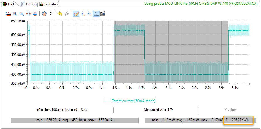
Reducing clock speed: 726 nWh
Now let’s see what happens if we reduce the clock frequency from 15 MHz to 1 MHz, using the Clocks Tool:
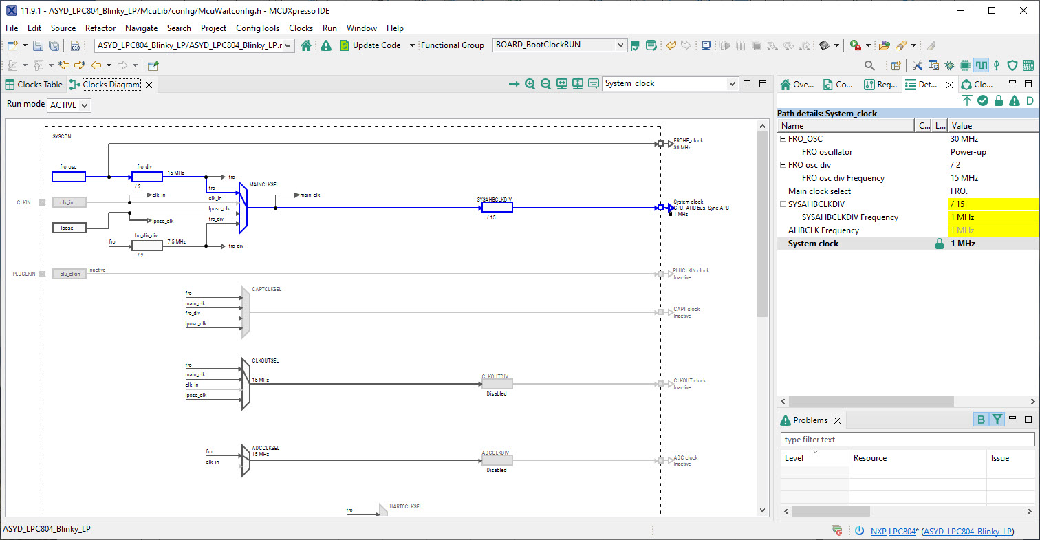
With this, the sorting and blink takes 15x longer (480 ms), but with the lesser current used with the slower clock, we still get a reduction down to 726 nWh:
💡 Takeaway: reducing the MCU clock speed helps reducing the energy needed. However, computation will take longer too.
RTOS with Sleep: 403 nWh
So far we have not used any low power mode, and were just waiting with NOPs. A much better way is to use an RTOS like FreeRTOS which cares about all the timing. With the following I enable the project to use FreeRTOS:
#define McuLib_CONFIG_SDK_USE_FREERTOS (1)
So I change my working loop into a simple FreeRTOS Task:
static void blinky(void *pv) {
  int arr[] = {0, 23, 14, 12, 9};
  for(;;) {
    LEDS_On(LEDS_GREEN);
    for(int i=0; i<500; i++) {
      selectionSort(arr, sizeof(arr)/sizeof(arr[0]));
    }
    LEDS_Off(LEDS_GREEN);
    vTaskDelay(pdMS_TO_TICKS(1000));
  }
}
Inside the FreeRTOS hook I enter the ARM Sleep mode with the WFI (Wait for Interrupt) instruction, whenever the system is idle. This assembly instruction puts the ARM core into sleep mode, with the clock to the core stopped (clock gating).
void McuRTOS_vApplicationIdleHook(void)
{
  /* Called whenever the RTOS is idle (from the IDLE task).
     Here would be a good place to put the CPU into low power mode. */
	__asm volatile("wfi");
}
With the WFI, the ARM core is not clocked any more (clock gating), and any interrupt will wake it up. In our case, the SysTick interrupt will wake us up.
With this, we get down to 403 nWh:
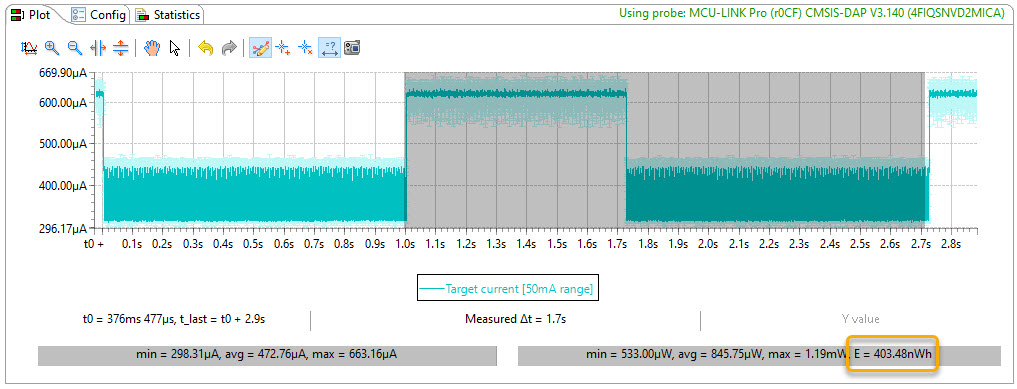
💡 Takeaway: using an RTOS, we can easily go into a low power mode with the RTOS knowing when the system is idle. The ARM SLEEP mode with WFI is a simple but effective low power mode clock-gating the CPU.
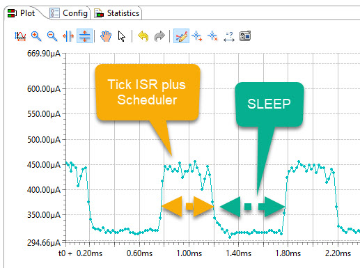
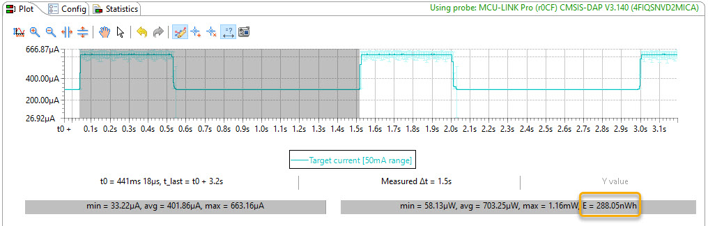
Reducing Tick Frequency: 307 nWh
So far the RTOS is running with a 1 kHz tick frequency: we leave the SLEEP mode every 1 ms, not leaving much time for the SLEEP mode:
With our timing needs, we can easily reduce the tick frequency to 100 Hz, still giving us a 10 ms timing. With changing the Systick rate to 100 Hz:
#define configTICK_RATE_HZ (100)
We get a reduction down to 307 nWh:
💡 Takeaway: reducing interruption from sleep mode can be managed by reducing the tick counter interrupt frequency.
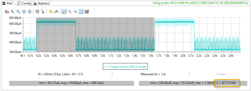
Tickless Idle Mode: 288 nWh
Can we get the ticks reduced even more? Yes, with using the FreeRTOS Tickless Idle mode. Because the RTOS knows about the scheduling, it can reduced the number of ticks, and there is a setting for this:
#define configUSE_TICKLESS_IDLE (1)
Enabling tickless idle mode, we get less interrupts and 288 nWh:
💡 To reduce further the tick interrupts by the RTOS tick counter, the tickless idle mode can be enabled. This further reduces the interrupts waking up the MCU from the low power mode.
Code Optimizations: 211 nWh
We saw earlier that the tick interrupt and scheduler needs a lot of time running at 1 MHz, and the same applies for the sorting time. Now it is time to optimize the code. I disable several things in the RTOS:
#define configCHECK_FOR_STACK_OVERFLOW       (0)
#define configUSE_TICK_HOOK           		 (0)
#define configGENERATE_RUN_TIME_STATS 		 (0)
#define configASSERT(x) /* nothing */
This alone would not help much, as we already have reduced the RTOS activity with reduced tick counts. So additionally I turn on -O3 compiler optimization plus disabling assert checks with NDEBUG. This all reduces the code size from 17 KByte to 8 KByte, so cut by half. With this, we get down to 211 nWh:
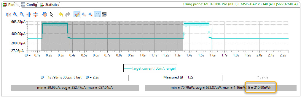
💡 Takeaway: we need to do the work as fast as possible, so we can go earlier into sleep mode. Compiler optimizations reduce the code size and speed up execution.
Low Power Timer: 162 nWh
Instead using the ARM Systick timer, we could use a low power timer, such as the WKT (wake-up timer) on the LPC804. Such a timer continues running in low power modes: something the Systick is not able to do.
On the LPC804, the WKT is running at 1 MHz and is powered by a LPO (Low Power Oscillator). We can enable it the following way:
#define configSYSTICK_USE_LOW_POWER_TIMER       (1) /* WKT Timer for LPC804 */
#define configSYSTICK_LOW_POWER_TIMER_CLOCK_HZ  (1000000) /* WKT runs with a fixed frequency of 1 MHz using the LP Oscillator */
In a ‘pre’ sequence it configures the wake-up source, disables the main clock clocks and switches to the FRO18:
void LP_PreEnterLowPower(void) {
  LP_ConfigureWakeUpSource(); /* enable deep sleep IRQ for WKT *

  /* switch main clock source to FRO18M */
  POWER_DisablePD(kPDRUNCFG_PD_FRO_OUT);
  POWER_DisablePD(kPDRUNCFG_PD_FRO);
  CLOCK_SetMainClkSrc(kCLOCK_MainClkSrcFro);
  CLOCK_SetFroOscFreq(kCLOCK_FroOscOut18M);
  /*CLOCK_SetFroOutClkSrc(kCLOCK_FroSrcFroOsc);*/
}
Then, depending on the selected low power mode, it enters it though an SDK call:
void LP_EnterLowPower(void) {
#if LP_LOW_POWER_MODE==LP_MODE_SLEEP
  POWER_EnterSleep();
#elif LP_LOW_POWER_MODE==LP_MODE_DEEP_SLEEP
  POWER_EnterDeepSleep(LP_ACTIVE_IN_DEEPSLEEP);
#elif LP_LOW_POWER_MODE==LP_MODE_POWER_DOWN
  POWER_EnterPowerDown(LP_ACTIVE_IN_DEEPSLEEP);
#elif LP_LOW_POWER_MODE==LP_MODE_DEEP_POWER_DOWN
  POWER_EnterDeepPowerDownMode();
#endif
}
With this, we can switch to the LPO clock during the sleep period, and we get down to 162 nWh:
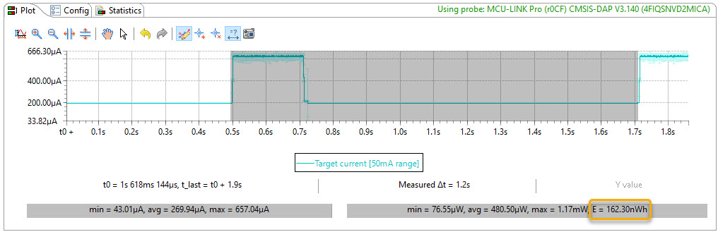
💡 Takeaway: the ARM Systick does not run in certain low power modes. Use a low power timer which still can run and wake-up the system as needed. Using a low power timer allows the system turn off more clocks and areas of the MCU.
Deep-Sleep: 115 nWh
With the low power timer active and able to wake us up, we can enter another low power mode: the Deep-Sleep mode. In that mode, the clock to the ARM Core is stopped as in the Sleep mode. In addition, all peripheral clocks are stopped except for the FRO or low power oscillator we already are using. Different interrupts (pins, UART, I2C, brown-out-detection, …) including the WKT can wake us up.
💡 WARNING: in Deep-Sleep the debug block is disabled too, making it impossible for the debugger to wake up the MCU. Use the safety belt from above!!!!!
Using DEEP-SLEEP we get down to 115 nWh:
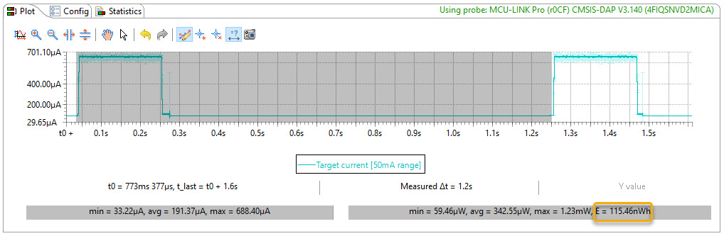
💡 Takeaway: lower power modes turn off more areas of the MCU, including the debug block. Using a safety belt is critical, otherwise the device might get bricked and lost.
Power-Down: 70 nWh
In Power-Down mode, the CPU, peripherals and clock sources are off, except the LPO (Low Power Oscillator). In addition, the flash clock and analog blocks are shut down. The LPO still can run, as well optionally the BOD (Brown-Out Detection). Interrupt wake-up sources need to be configured through special wake-up configuration registers. With everything from above in place, I can use FreeRTOS with the WKT and get down to 70 nWh:
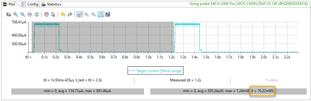
As an interesting detail: we have reached the bottom of what the MCU-Link Pro is able to measure 🙂 :
Deep-Power-Down?
There is yet another low power mode available, the Deep-Power-Down. However, in that mode, only a ‘Wakeup’ pin can be configured and used as wake-up source. This makes it a great mode for applications which can wake-up with a user button, but it is not applicable for our application here, so not used.
Work fast, sleep early: 10 nWh
So far the core is running at 1 MHz. As a general rule: in low power applications you want to do the work fast, then go to sleep earlier. So let’s switch back to 15 MHz and we reach 10 nWh:
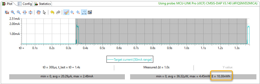
The ‘work fast – sleep early’ approach works even better if one has to work on a periodic base.
💡 Takeaway: ‘work fast & sleep early’ can be a good approach, but depends on the type of application. It increases the peak current, which could be a problem for the power supply.
Summary
We have touched on the topic power and energy, and what are the variables we can deal with.
We have used multiple and different approaches: changing clock frequency and supply voltage, implemented clock gating for core and peripherals, using low power clocks and timer, up to optimizing the application so it can perform the work faster and go to sleep earlier, with the use of sleep and low power modes.
I think it has been an impressive journey for our (admittedly) simple application: from 2390 nWh down to 70 nWh for a working cycle, and this with running FreeRTOS! Not bad for basically doing the same thing, but optimized for low power and low energy.
Here again the numbers from the measurements:
You can find the project used in this article on GitHub.
Happy powering 🙂

Terrific tutorial, very well explained and speckle-less!. Well done Erich!
LikeLike
Thank you!
LikeLike
Eric
LikeLike
Hi Robert, message sent to early?
LikeLike
Erich:
Great article (as always)!
I recently bought a Joulescope JS200 Precision Energy Analyzer for precise power / energy measurements (https://www.joulescope.com/products/js220-joulescope-precision-energy-analyzer). At US$999, it’s much more expensive than your elegant setup, but it spans six decades of dynamic range (down to nanoamperes), measuring 2 msps 16-bit, simultaneous current and voltage. It also accepts GPIO inputs which you can use to “label” various phases of computation on their excellent GUI.
Not every project needs the speed, precision or dynamic range of the Joulescope, but it has become a staple in my low-power project development.
(Note: I don’t receive any compensation for this endorsement – I just think it’s an excellent tool.)
Best,
— rdp
LikeLike
What I’m using otherwise is a Otii Arc from Qoitech (same for me, I don’t receive any compensation for this endorsement 🙂 ). Costs around $1000 and is an excellent tool too.
LikeLike
For a small budget I can recommend the Power Profiler Kit II from Nordic Semiconductor. I use it for my low power projects and it’s very useful for current measurements down to 1uA (the resolution is about 200nA)
LikeLike
Hi Christoph,
I’m using the Nordic Power Profiler II too: comparable with the MCU-Link Pro, with the plus of having a power source, but does not include a debugger. The PPK2 is a little bit more expensive (around $85), but a great tool and lots of value for the money, including logic analyzer pin. And I love the color LED’s on it :-).
LikeLike
Great details, interesting … on the other hand our controllers connect to 24V batteries capable of running 200A motors, our runtime current of maybe 60mA (300mW) is negligible! 🙂
LikeLike
Hi Ian,
yes, always a point of perspective and where the leverage point could be. The trade-in is about safety: here you want to make sure that things are robust and always works, so having a 5V logic and supply makes a difference to a 1.1V supply voltage, for example. Trading in more energy for more robustness?
LikeLike
Yes for sure … our switch inputs for example draw 20mA each because we want low resistance to protect from moisture problems!
LikeLike
These 20 mA are probably well spent :-).
LikeLike
I enjoyed reading your journey to lowest power. Reminds me of my struggles with the LPC804 and LPC845. It really is a “simple MCU” with many compromises and gotchas.
Tip: If you need to wake up periodically to check for some condition, and if you can check it within the LPTMR ISR, then SCB_SCR_SLEEPONEXIT can skip exiting from the ISR if you just want to go back to sleep. It can save a few cycles. (but I guess it’s not applicable to your trivial example with an unconditional wake-up)
LikeLike
Hi Paul,
thanks. And yes, these MCUs are not the most complicated ones, but still have challenges and tricks as the one you mention about the SCB_SRC_SLEEPONEXIT.
I have looked at this one for the labs and this ‘test’ application, but unfortunately it is not applicable. Maybe I should change some of the boundaries and parameters of the labs for this.
LikeLike
I like this lots.
Two things I do to save power are.
Tickless timers are essential. For that you need to be able to read the time since whenever on the fly and use that to calculate the next wake up interrupt delay. So you can sleep as deep as possible without a tick timer always waking you up.
The other is a set of flags that you can set for each peripheral to indicate the deepest sleep state allowed. So is a peripheral needs the high speed clock you set that flag. So when the lowest priority task handles timers and calls sleep will leave it on.
If you’re being sleezy like me and call blocking delay_ms() type functions inline you can also use the min sleep mode to go to sleep while waiting.
Advice: When designing low power products implement the low power stuff first. Because retrofitting it later is painful and will cause problems, like battle tested code randomly fails in hard to figure out ways.
LikeLike
Yes, tickless timers are a great way to reduce the wake-up time. About the delay_ms() or equivalents, it is always good to check how it is implemented, and depending on that implement your own routine.
LikeLike