
For more than two years I’m using the NXP LPC845 in my university courses. Beside of that it is used in many projects. First, because the LPC845-BRK board is small, breadboard friendly and inexpensive. Second, for many small projects that Cortex-M0+ provides just the right amount of processing power and memory.
If you search for ‘LPC845’ on my blog, you will find many articles about it. We are using the LPC845 in a research project, and one developer asked me why the LPC845 seems to run slower than expected. And I was sure that I wrote already an article about this, but to my disappointment: even Google did not find it? So complete this unfortunate gap, here is it: how to optimize the LPC845 and running it at full speed, with the hand-brake released.
Problem
So what is the problem? You might notice it if you are implementing a real-time synchronization with ARM NOP (no-operation) instructions:
__asm("nop");
If I run this on the usual ARM-Cortex devices, execution will take 1 CPU cycle. So on a 18 MHz (core clock) part, it will execute 18 million NOPs in a second. But not on a LPC845: it takes takes more time, or more precise: a NOP needs three cycles! First I thought there must be something wrong with my clock settings, but all the other things like timers were running at the correct speed. Just code execution was slower than expected.
Here is a simple test program to measure the timing:
static void test(void) {
  McuGPIO_Config_t config;
  McuGPIO_Handle_t gpio;

  McuGPIO_GetDefaultConfig(&config);
  /* PIO0_00 */
  config.hw.gpio = GPIO;
  config.hw.port = 0;
  config.hw.pin = 0;
  config.hw.iocon = IOCON_INDEX_PIO0_0;
  config.isHighOnInit = false;
  config.isInput = false;
  gpio = McuGPIO_InitGPIO(&config);
  McuGPIO_Toggle(gpio);
  for(;;) {
    GPIO_PortToggle(GPIO, 0, (1<<0));
    GPIO_PortToggle(GPIO, 0, (1<<0));
    GPIO_PortToggle(GPIO, 0, (1<<0));
    GPIO_PortToggle(GPIO, 0, (1<<0));
    GPIO_PortToggle(GPIO, 0, (1<<0));
    GPIO_PortToggle(GPIO, 0, (1<<0));
    GPIO_PortToggle(GPIO, 0, (1<<0));
    GPIO_PortToggle(GPIO, 0, (1<<0));
    GPIO_PortToggle(GPIO, 0, (1<<0));
    GPIO_PortToggle(GPIO, 0, (1<<0));
  }
}
It initializes the PIO0_00 GPIO pin, and then toggles it as fast as possible in a loop. To not count in the loop overhead, it toggles it 10 times.
The assembly code confirms that a toggle just is one instruction:
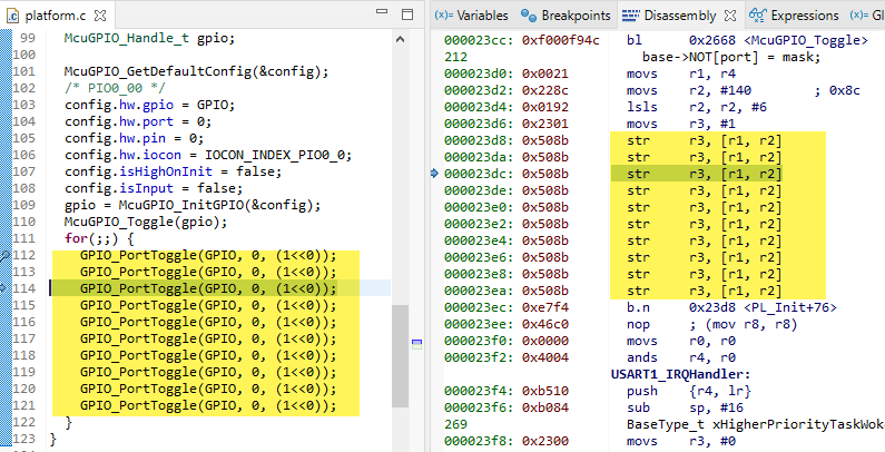
The instruction is a
str r3, [r1,r2]
which should take two cycles (1 for instruction and one for the memory access). So we should see the pin toggling at half of the core clock, in my case with 9 MHz.
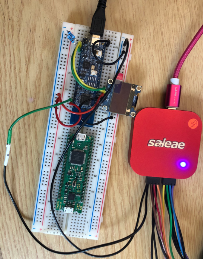
Measurement is with a Salea Logic Analyzer with 250 MHz sample rate.
And the result is interesting: It is slower than expected, plus each toggle does not take the same time:
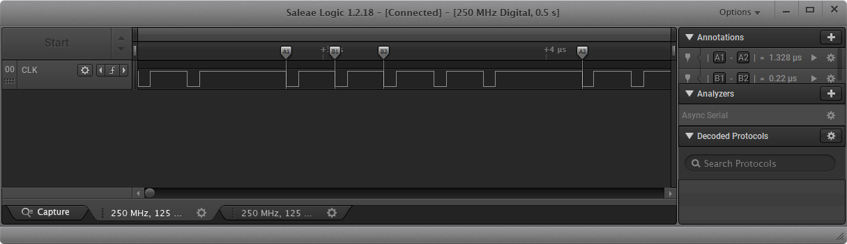
The loop takes 1.328 us. Two toggles take a total 0.22 us. And not the expected 0.11 us. Why the toggling frequency is not constant, is not fully clear to me.
What could it be? If the core is executing at 18 MHz, it should execute the instructions at that speed, plus of course the extra cycle for the memory store. Except: if something else is slowing it down. For the NOP it needs to fetch it from memory, decode it and then execute it. For the store, there is a fetch, decode, execute with a store. Decoding and executing depends on the CPU core clock, but fetching depends on the memory. And this is the problem here: memory reads or fetches are not performed in a single cycle, but slowed down. The code is executed from FLASH memory, and obviously there are some wait states present here.
Flash Configuration Register
A bit of searching in the reference manual reveals this:

With this, it makes now sense: the default is 0x2, so each flash memory access takes 3 system clocks, slowing down not only flash memory read, but as well execution of instructions fetched from that memory.
Solution
So here is a solution to ‘fix’ it:
static void setFlashWaitStates(uint8_t nofWaits) {
  /* Configure the FLASHCFG with the FLASHTIM (Flash memory access time).
   * Latest NXP SDK provides the function IAP_ConfigAccessFlashTime() to do a similar thing.
   * By default after reset, the LPC845 sets it to 0x2 which is 3 system clock access time.
   * NOTE: if getting for higher clock speeds a hardfault, then add some wait states. The LPC845 just runs fine with zero wait states and maximum clock speed for me :-).
   */
  uint32_t val;

  val = (FLASH_CTRL->FLASHCFG)&~FLASH_CTRL_FLASHCFG_FLASHTIM_MASK; /* do not touch the other bits! */
  switch(nofWaits) {
    default:
    case 0: val |= 0x0; break;  /* 1 system clock access time */
    case 1: val |= 0x1; break;  /* 2 system clock access time */
    case 2: val |= 0x2; break;  /* 3 system clock access time */
  }
  FLASH_CTRL->FLASHCFG = val; /* write back settings */
}
I call it with 0 for zero wait states (it still needs one cylce to access the memory), and voilà: now it runs at the expected speed. As noted in the comment: for higher clock settings this might be too fast, but it is worth to try it out.
And as noted: the NXP SDK has recently added a function to configure the wait states too:
void IAP_ConfigAccessFlashTime(uint32_t accessTime)
{
    uint32_t temp;
    temp = FLASH_CTRL->FLASHCFG;
    temp &= ~FLASH_CTRL_FLASHCFG_FLASHTIM_MASK;
    FLASH_CTRL->FLASHCFG = temp |  FLASH_CTRL_FLASHCFG_FLASHTIM(accessTime);
}
Personally, I think the first implementation is better, but maybe it is just me.
Regardless, with setting the value to zero, I get the performance which I expect:
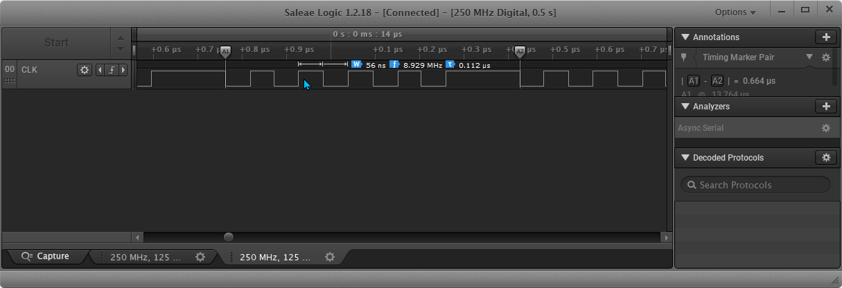
One loop takes now only 0.664 us, with a (symmetrical single toggling time of 56 ns or the 9 MHz I expect.
Testing with NOPs
I did create another test case, this time just toggle between 10 NOPs:
  for(;;) {
    GPIO_PortClear(GPIO, 0, (1<<0));
    __asm("nop");
    __asm("nop");
    __asm("nop");
    __asm("nop");
    __asm("nop");
    __asm("nop");
    __asm("nop");
    __asm("nop");
    __asm("nop");
    __asm("nop");
    GPIO_PortSet(GPIO, 0, (1<<0));
  }
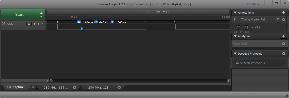
With the default settings (3 system clocks flash access time) it needs 1.164 us for the 10 NOPs between the pin toggles: clearly the NOPs are executed with about half of the system core clock time:
With zero wait states (1 system clock flash access time) it takes 0.608 us: here the 10 NOPs need the expected 0.55 us plus the time for the pin change:
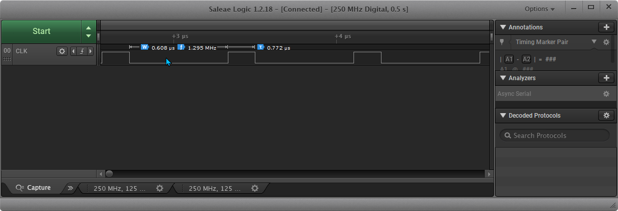
Now the NOP instructions are executed at the speed of the clock, which is what I want and expected :-).
Summary
It is not clear to me, why on the NXP LPC845 the default is using such a conservative and slow flash timing. At least for the LPC845 I’m able to run it with zero wait states (1 system clock flash access time) at max core speed. Regardless what ARM Core and device you are using: it might be worthwhile to measure execution time from FLASH. If you measure slower than expected values, it might be worthwhile to check your device reference manual if there are any settings for memory access you could tweak. Of course carefully read the information and test it. But at least for my case I can say that I’m able to run my LPC845 projects with zero extra flash wait states added.
I’m not clear why the toggling with the waits inserted creates that non-symmetrical pin toggling: I would expect the pin toggling slowed down equally, and not some toggles faster than others? If you know the answer or possible explanation, I want to hear about it, so please post a comment.
Happy tuning 🙂
Links
- Tutorial: Blinky with the NXP LPC845-BRK Board
- Unboxing the NXP LPC845-BRK Board
- LPC845-BRK Board web page: https://www.nxp.com/LPC845Breakout
- User Guide for LPC845-BRK Board: https://www.nxp.com/docs/en/user-guide/UM11181.pdf
- NXP LPC845 web page: https://www.nxp.com/products/processors-and-microcontrollers/arm-based-processors-and-mcus/lpc-cortex-m-mcus/lpc800-series-cortex-m0-plus-mcus/low-cost-microcontrollers-mcus-based-on-arm-cortex-m0-plus-cores:LPC84X?

Hi Erich,
there is post on NXP community addressing the flash access time on LPC845.
https://community.nxp.com/t5/LPC-Microcontrollers/LPC8xx-Flash-access-time-aka-setting-FLASHTIM/m-p/1186229
Generally speaking flash is usually set for worst case access time (temperature, manufacturing tolerances,…etc). So your setting may work reliably at room temperature, but when you heat up device to 105 you may experience hard faults like other customer here.
https://community.nxp.com/t5/LPC-Microcontrollers-Knowledge/TN005-Heat-LPC11U68-and-reset-it-will-enter-hardfault-docx/ta-p/1129177
Regards Petr
LikeLiked by 1 person
Hi Petr,
thank you so much, this is really important information, and at least gives some clarity about the temperature. But I did not find that 105 number anywhere? Is that Celsius (which I assume) or Fahrenheit? And it is not clear to me if and how much the LPC11U68 is the same or similar to the LPC845? Maybe I wrongly assumed that the LPC845 is different or newer.
LikeLike
Hi Erich,
it was just example what can happen in corner cases if you have too tight flash settings. The operating temperature range for LPC845 is -40°C to +105°C. The LPC845 is of course newer, but AFAIK its on the same technology node with the same flash as LPC11xx.
LikeLiked by 1 person
Hi Petr,
thanks a lot, this makes now sense. I think it makes sense for a conservative default setting, but I assume very few applications might get up to that +100 degree area. For anything going up beyond 85 degree C I always prefer to use automotive rated parts (AEC-Q200 grade 0, which allows to run the part from -50 up to +150 degree C), or at least using grade 1 (-40…+125 degree C)).
LikeLike
I do dislike those format NXP documents; I wasn’t able to see anywhere that specified the Flash speed, it’s possible the flash can’t read at full ARM speed (surely it’s documented somewhere).
Slowing flash and therefore execution also reduces current consumption.
The erratic timing with delay cycles hints at some small cache in the flash (again, can’t see in docs anywhere)
LikeLiked by 1 person
Hi Ian,
thanks for your comment. I don’t think the extra delay is to reduce current consumption. Most applications have less overall energy consumption if they can get to sleep mode faster, and here code execution takes longer. It basically holds off the CPU.
Me too, I was thinking that there could be a small cache somewhere, but as you noticed: did not find anything about it.
As for the extra wait states: I believe this is set in the ROM boot code. And if I’m not mistaken, I have seen older LPC parts with ‘older’ FLASH technologies (LPC parts are around for a while, and were introduced earlier than the Kinetis parts), so it could be that the extra waits were necessary for these technologies?
LikeLike
typically, flash access speed is limited to about 20MHz. So at max speed of 30MHz, you should add one wait state. This 20MHz could be higher with smaller process geometries, and might work with zero wait states. But not over temperature–so add 1 wait state to be sure.
Also, the M0+ Kinetis parts have better documentation and will run at 48MHz.
LikeLiked by 1 person
Hi Brad,
thanks for the comment about that ~20 MHz Flash speed. So the LPC845 running below 20 MHz really should not need to add a wait state. I get that point about over-temperature, but did not find any documentation about this or where the boundaries are? I really wish things like that would be better documented, so I hope this article at least raises some awareness.
LikeLike
Nice analysis of the memory operation.
Thank you!
LikeLiked by 1 person
Thank you. I’m still puzzled why the default adds the extra waits and why the toggling time is not equal. But did not find anything in the documentation.
LikeLike
Most likely it’s a worst case situation – putting in the extra waits means that the board will run properly at all clock speeds rather than adding extra documentation (that nobody new to the board will read) that explains that it’s required when running faster than the default speed.
Good job as always.
LikeLiked by 1 person
Yes, I agree that this will deal with the worst case situation.
The SDK comes with a SDK_DelayAtLeastUs() which assumes that instructions will be executed with no extra delays. Well, it says ‘at least’ which turns out it will be ‘at least twice as double’ with the default settings. Which is of course on the safe side too :-).
LikeLiked by 1 person