
The NXP Freedom boards are very popular. Many of them are inexpensive (less than $20), include a debug interface and can be easily extended with extra shields or boards. Especially the FRDM-KL25Z is very popular: I’m getting told because of Processor Expert and tutorials available on web sites like this one ;-).
Unfortunately there are no small or breadboard friendly Kinetis boards available. There is the NXP LPC800-DIP but with no onboard debugger and without Processor Expert support. We have the tinyK20, but projects tend to use more CPU power, FLASH and RAM space than what the tinyK20 board (50 MHz, 128 KByte FLASH, 16 KByte RAM) can provide. So we ended up designing the big brother of the first tinyK20: the tinyK22 with 120 MHz, 512 KByte of FLASH and 128 KByte of RAM.
tinyK22 Overview
While the Freedom boards are great, they are not ideal for wearable, bread boarding, small projects or where low power/battery operation is required. What we need is a small board with an onboard debug interface and a capable processor, similar to the STM32 Nucleo-32 boards which are both small and inexpensive. Plus the board needs to be used used with industry standard Eclipse and JTAG/SWD tools (sorry, no Arduino!).
Instead making our own boards, we considered buying the excellent Teensy 3.5 boards. The problem with the Teensy boards is that you cannot debug it with a normal SWD/JTAG debugger, and it uses a proprietary loader. While the Teensy can be hacked (see “ Search Modifying the Teensy 3.5 and 3.6 for ARM SWD Debugging“), it means higher costs plus an external debug probe is needed. What we want is a user friendly, industrial grade and open source tool chain and not yet another Arduino environment.
Similar to the tinyK20, the board is breadboard friendly. As a plus the board can be directly soldered on a base board using the outside PCB solder rings. Below is the first ‘hand hand-produced’ prototype board:
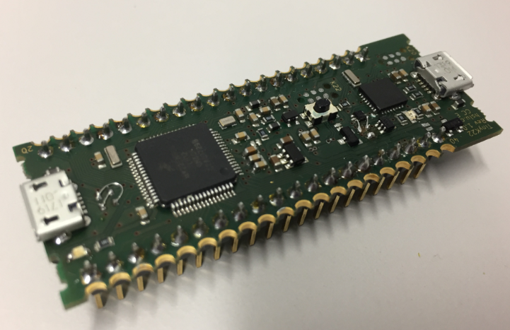
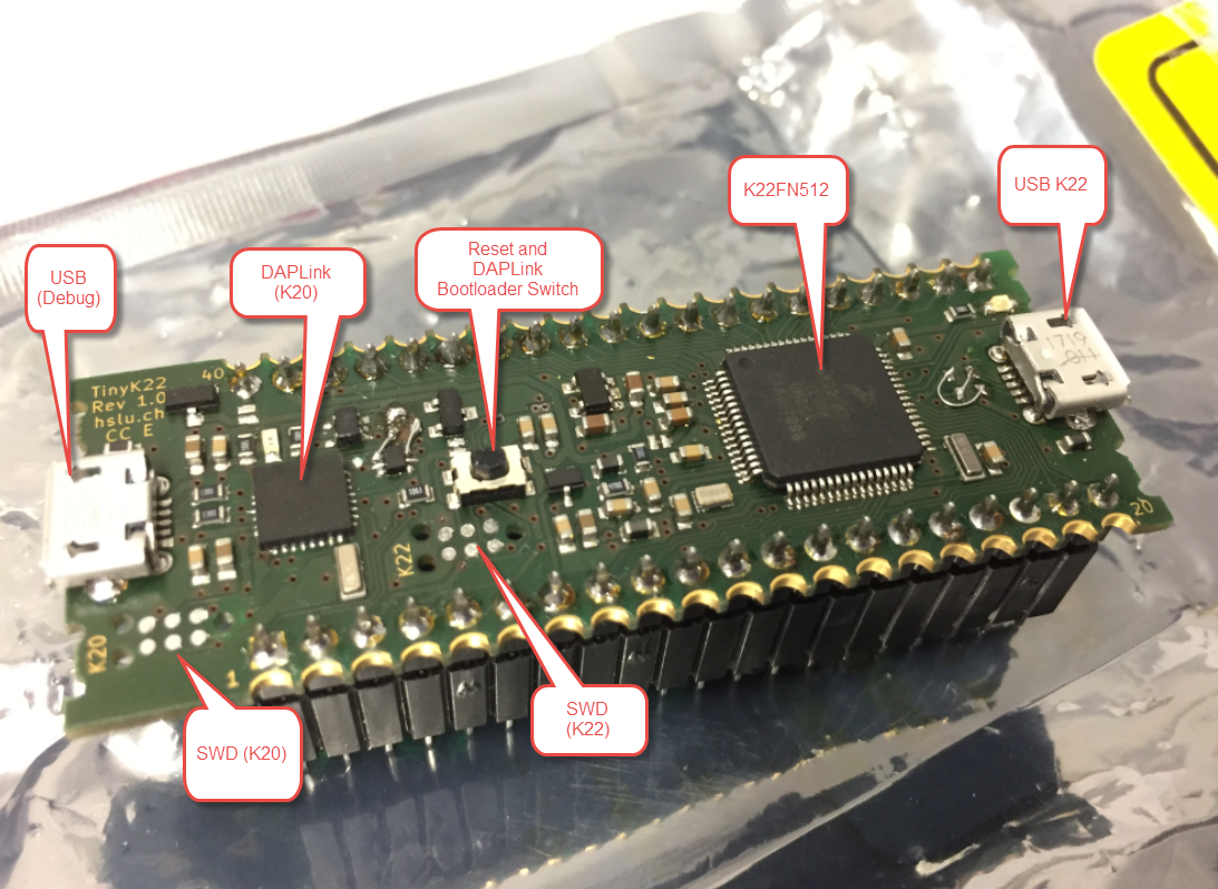
tinyK22 top
On the board there is a NXP K22FN512 (same device as on the FRDM-K22F). The K22FN512 (120 MHz ARM Cortex-M4F) has more FLASH (512KB) and RAM (128 KB) than the K20DX128 (50 MHz) on the tinyK20 (128 KByte FLASH and 16 KByte RAM). But main decision factor for the K22F was that it is supported by Processor Expert.
The board includes the Kinetis K20 which is loaded with the DAPLink bootloader and CMSIS-DAP debug firmware: that way no external debug interface is needed. The K20 DAPLink device can be disconnected if needed. For first programming of the K20 and K22, the board includes PCB top layer contact points:

SWD Debug Connections
That way no expensive connectors are needed, and the holes in the PCB are used to align the probe and fix it from the bottom side with an adapter if needed. The picture below shows the needle adapter with the backside fixing part. Other variants of such adapter can be found e.g. on http://www.tag-connect.com

Debug Needle Adapter
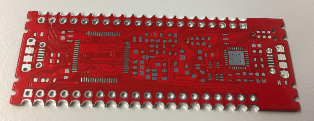
As the tinyK20 (see “Data Logger with tinyK20 Board“) the board has the option to add a micro-SD card socket on the PCB bottom side. If the SD card is power-hungry, an extra 3.3V regulator can be added as the K22 can only provide about 100 mA with it internal regulator.

tinyK22 bottom
The first prototype is working fine, and we are going to make a small test batch in the coming weeks, followed by a larger volume one probably early next year. Target costs for around 200 boards is around or less than $20.
Below images from the second run with a few fixes applied: boards produced in China without gold plating:

Red TinyK22 populated
Red TinyK22 top layer

Red TinyK22 bottom layer
If there is enough interest and demand, we could consider to make the design/board available outside of the university: what do you think?
Happy Breadboarding 🙂
PS: Thanks to Christian Di Battista for this great design!

The whole tinyKxx concept is great, i like the rings at the edge of the PCB on this one.
It might be a nice addition for my dev board collection 🙂 but i don’t know how much the shipping cost is compared to the cost of the board (i’m in latino america).
PD: Thanks for your commitment on the blog, it’s a great learning source 🙂
LikeLike
Cool to see someone else using the TC-2030 connector. I’ve been using those for years with BDM devices, though they’ve never come out with a BDM version and I had to make up my own pinout and adapters. My only complaint now is that the strain relief doesn’t hold up that well over time and the cables cost me $50 each to replace.
If you’re really tight on board space, you can grind the alignment pins down and put the pads on the back side of the board from the MCU. It’ll fit diagonally under an LQFP-64.
I might buy a couple of the boards if they were made available.
LikeLike
Ah, thanks for mentioning the connector name (it did not come to my mind when writing the article). Yes, the cables are not cheap, but space and part costs on the board was a concern. BTW, SEGGER has these connectors on their boards too (e.g. the bigger one on https://jaycarlson.net/2017/08/18/make-j-link-less-annoying-two-wire-3-3v-power-fix/) or the same 6-pin one on the J-Link EDU version. We had as well an idea to use a 3D printed alignment adapter (clicking on the sides of the board) so we could save the holes for the alignment. That way it would not need access on the back side to firmly attach the cable.
LikeLike
I’ve found the fine-pitch pads to be hard to build fixtures for. Not that I’m much good at building fixtures. I did have one fixture built with pins for a TC-2030, but after that I added larger test pads next to the important pins to make easier targets for pogo pins.
Also, if the boards are v-scored or have perforations it’s harder to locate accurately off of the sides.
LikeLike
All is well. Only in vain they put the plug “micro-usb”.
LikeLike
We had discsussion about using mini vs. micro USB. I agree that the mini is more robust. But on the other end students have more micro USB cables available than mini USB, plus the connector is smaller. So we decided for the micro and with this we can assume everyone already has a cable. Otherwise we would have to supply extra cables. We have other boards with micro USB connectors, and that worked fine so far.
LikeLike
Yes, yes. One unsuccessful move, we throw out the board.;-))
LikeLike
I would buy one.
LikeLike
I interested in buying one
LikeLike
Same!
Would love to see them commercialized or the design released.
LikeLike
Thanks for the feedback. So far we passed some of the boards to other universities, but so far this did not justify a larger production run yet. To make it available to the external world is just extra efforts for which we don’t have resources yet. But hopefully this can change early next year, lets keep fingers crossed.
LikeLike
Good Job! Just some suggestions from my side:
From the bottom side of the PCB the microUSB receptacle seem to have a shell-through-hole tab in order to give them more robustness. This would cause interference between SDcard and the soldered tabs. In this case, you can consider to move to a fully SMT shell receptacle.
Another drawback is the SWD (K22) almost in the middle of the board. In a debug scenario, to use the clips to retain the probe you have to unplug the tinyK22 from the mainboard, clip the probe and plug the tinyK22 again (praying the clip wont be released…). One option could be swap SWD connector (K22 K20) as K20 should not be used regularly. For me, the best option is to use the Legged version of Tag connect.
Finally, edges plating are nice but in this scenario (tinyK22 soldered to a mainboard.) you wont be able to plug any miniUSB cable to their receptacles. To do this you should solder the tinyK22 close to mainboard edges…Never in the middle.
LikeLike
Hi Gaston,
many thanks for your suggestions! I’ll check if we can use SMD USB connectors instead (again, the concern is that students might rip them off the board too easy).
The K22 SWD is supposed to be there only in the of kind of ’emergency’ (e.g. if the DAPLink is not able to get access to it). Hopefully it never is needed. In that case it would be OK to hold the debug probe on the contacts or use another fixing method. What is the ‘legged version of Tag-Connect’ for you? the one with the holding clips? I’m affraid that that one needs too much space. You are right that if the board gets soldered on another one, it is best if the board is on the edge. Maybe there are low profile micro USB cables too?
LikeLike
About the USB connector and the SD card: why do you think there will be interferences? The through hole connectors should not reach the bottom of the PCB, and they are GND only? I’m missing something?
LikeLike
Okay, they don’t reach the bottom of the PCB but they are intended to solder them, adding solder material to the bottom side. Or you plan to leave them unsoldered? Regarding the other questions: Yes, the legged version comes with the holding clips and certainly too big for this application… I agree with you it is not necessary as the connector is used in case of ’emergency’. I also think a low profile USB cable could be used when plating edges are soldered to the mainboard.
LikeLike
All parts are hand soldered right now, and currently it does not reach the bottom of the page. But yes, that might be differnt in the production version.
It does not (or should not) conflict with the SD card, as with the SD card spring contacts, the card has a little space between the card and the PCB.
Anyway, the goal is to have the bottom side of the board flat, so it could be soldered directly on another board (with an isolation sheet between the PCB’s, just in case).
LikeLike
Hi Mr. Styger,
For me it would be awesome to have this board! 🙂
But if I could request, it will be more awesome if you could make some tutorials of how to start with this board and ARMs.
I have followed you blog since 2013 when I understood that Arduino hides me to many things and I decided to change to ARM. But i never do it (I’ve only made a few attempts) 😦
Over all this years there have been so many changes… In the companies, IDEs, SDKs, programing firmwares, new MCUs… This and the limited information available (compared to Arduino) makes it difficult to me to do the jump to ARM.
But I think that this board is an opportunity for me to start from zero 🙂
One question, it could be possible to program and debug other devices with the onboard DAPLink?
Thank you very much for this fantastic blog!
LikeLike
We thought about adding the ability to debug another board with it. But it would require too much space, parts and costs, so we did not add that capability. Because for $20 you can get a Segger EDU.
LikeLike
Hey Erich, do I spot some patch wires?!
Glad that you used micro-USB connectors with through-hole studs, otherwise the connector peels off the board easily (I have a pile of Microchip dev boards with peeled-off micro-USB connectors).
Looks good!
Best Regards, Dave
LikeLike
Yes, that’s a patch wire. We had to fix a small thing. I’ll post a picture of the new PCB if I can today.
LikeLike
FYI, I have added pictures of the new ‘red’ board to the original article.
LikeLike
Pingback: MCUXpresso IDE V10.1.0 with i.MX RT1052 Crossover Processor | MCU on Eclipse
Pingback: New Concept for 2018 Mini Sumo Roboter | MCU on Eclipse
Hi there,
I have a similar board, the MiniMoon.
MK22FN512VLH12 microcontroller, but only programmable with JTAG connector.
All pins, but the crystal and USB ones, are available (2×25 pins board).
Regulators for 3.3V and 5V integrated.
It offers the bare system, so you can use it as you want.
You can take a look at it here (in Spanish):
http://www.elektroquark.com/wp/2017/07/06/quark-lxx-modulo-de-desarrollo-para-kinetis-minimoon/
Design files will be available soon.
LikeLike
Congratulations, that’s a neat and cool board! Thanks for sharing!
LikeLike
Pingback: tinyK22 Boards arrived | MCU on Eclipse
Great Job! Erich! it gives an motivation to others keep doing projects with NXP.
LikeLike
I have to say that the supply for the parts have been a challenge and a big risk. We were lucky to get enough microcontrollers from the distributors, but I know others were not so lucky. I really hope that this supply problem will go away soon, as it starts impacting many projects.
LikeLike
Pingback: Flash-Resident USB-HID Bootloader with the NXP Kinetis K22 Microcontroller | MCU on Eclipse
Pingback: Reverse Engineering of a Not-so-Secure IoT Device | MCU on Eclipse
Pingback: Building and Flashing ESP32 Applications with Eclipse | MCU on Eclipse
Pingback: Building a Raspberry Pi UPS and Serial Login Console with tinyK22 (NXP K22FN512) | MCU on Eclipse
Pingback: Tutorial: Maximum Clock Frequency for Kinetis using MCUXpresso Clock Tools | MCU on Eclipse
Pingback: tinyK22 Board Rev 1.3 released | MCU on Eclipse