
Newer microcontroller have increase RAM areas, making it suitable to run the application from RAM instead of FLASH. For the FRDM-K64F board and the Kinetis Design Studio (V1.1.1), I have explored how to run the application out of RAM instead of FLASH memory, both for P&E and Segger connections.

MK64FN1M0VLL12
Why a RAM Configuration
My engineering principle is: an engineer should develop in an environment which is used later in production (see “Debug vs. Release?“). Simply because if you develop and debug what the product will be, you have a better chance to catch errors early. The same thing applies to RAM or FLASH targets. With RAM targets the code and application runs in RAM, while with FLASH it runs out of FLASH memory. In the early days of microcontroller FLASH technology, the FLASH erase-program cycles were limited: my first microcontroller allowed to reprogram the FLASH only 50 times! So it made sense to start developing in RAM first, not to wear out the FLASH memory too early. Another advantage (in the past) was that downloading to RAM was faster than to FLASH. But with the faster FLASH and debugging probes this is not much a need any more. Other than that: running the program out of RAM memory might be faster, to increase the application performance.
The K64F on the FRDM-K64F board has 256 KByte of RAM, so it is possible to run rather large programs out of RAM.
❗ The memory on the Freescale Kinetis-K devices is *not* continuous! There is a memory barrier at 0x2000’0000 which segments the memory, so you cannot use that memory in one single piece! See “FreeRTOS Heap with Segmented Kinetis K SRAM“.
Downloading and debugging a RAM target is rather easy with Kinetis Design Studio and projects created with Processor Expert.
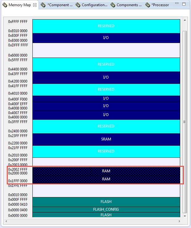
256 KByte RAM of K64F
Using a RAM Configuration
The wizard creates a project with both a RAM and a FLASH configuration, with the FLASH set as the default (see “Configurations with Processor Expert“):
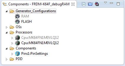
Processor Expert Project for FRDM-K64F
To switch the configuration, I select it and use the context menu:
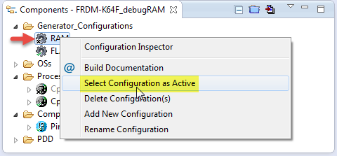
Selecting Configuration
This makes the RAM configuration active. Note that a different CPU is now selected in this configuration:

Selected RAM Configuration
The difference to the FLASH target is that in the Build options of the CPU all the code and data gets placed in RAM areas:
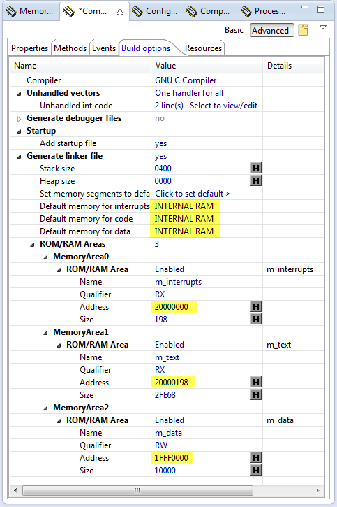
Code and Data Placed in RAM
Therefore, the generated linker file is using RAM areas too, and places code and data in RAM, with the exception of the FLASH configuration and protection area (CFMPROT):
MEMORY {
  m_interrupts (RX) : ORIGIN = 0x20000000, LENGTH = 0x00000198
  m_text      (RX) : ORIGIN = 0x20000198, LENGTH = 0x0002FE68
  m_data      (RW) : ORIGIN = 0x1FFF0000, LENGTH = 0x00010000
  m_cfmprotrom  (RX) : ORIGIN = 0x00000400, LENGTH = 0x00000010
}
Debugging in RAM
P&E
Debugging a RAM configuration with the P&E connection is the same as using the FLASH configuration, no other changes needed:
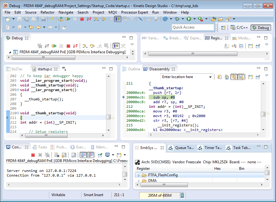
Debugging in RAM with P&E
Segger
If using the Segger J-Link connection, then have to disable the ‘Pre-run reset and halt’ in the debug/launch configuration:

Segger Debugger Launch Configuration to Debug in RAM
With this, I can download and debug in RAM:

Debugging in RAM with Segger
OpenOCD/CMSIS-DAP
Same for the OpenOCD connection: I need to disable ‘Pre-run reset’ in the debugger lauch configuration:
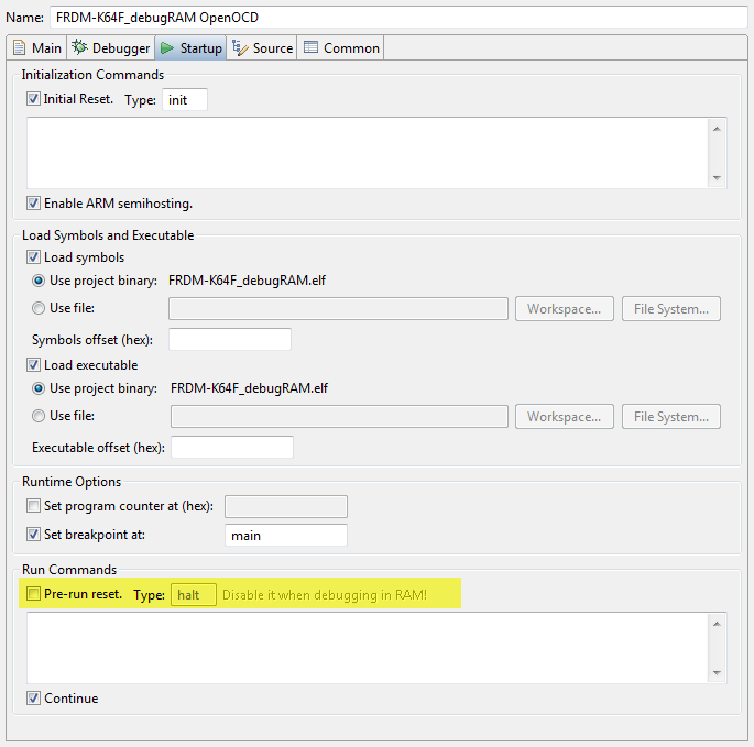
Debug Configuration for Debugging in RAM with OpenOCD
With this, debugging in RAM works:
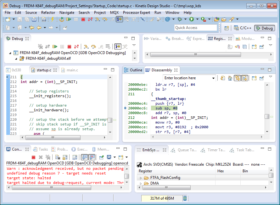
Debugging in RAM with OpenOCD
Summary
If you have enough RAM, it *might* make sense to run your application and to debug it in RAM. This means that in the linker file the code and data needs to be placed into RAM. I’m of the opinion that you should debug what you intend to build, but if you insist on debugging in RAM, hopefully this article helps you. And do not forget: if you power off the target, your application in RAM is gone 😉
Happy RAMing 🙂

Eric
I think you missed one quite big advantage of debugging in RAM – the number of breakpoints possible. Flash breakpoints are HW breakpoints limited to what the device supports (Kl parts have about 2 and K parts have about 4). RAM breakpoints are SW breakpoints and are virtually unlimited.
I admit to personally not really using RAM debugging. In fact I rarely use Flash debugging since I simulate the Kinetis so don’t need to debug on the HW very often. However, when providing solutions for other users one needs to accept that some users want to be able to do things “their preferred way” and so it is important to be able to provide a solution for them; whether is is to be able to work on a MAC, under Linux, with Keil, IAR, Atollic, CooCox, CW, KDS etc. or use a RAM target it is good to be able to provide them with this rather than restrict them to a limited set.
Regards
Mark
LikeLike
Mark,
The 4 hardware breakpoints on the Kinetis K are sufficient in my view for most use cases. The 2 on the L series is more challenging, but usually works out ok. For debugging the L parts and when I need more breakpoints in FLASH, then the Segger feature https://www.segger.com/jlink-unlimited-flash-breakpoints.html helps me out. For that small devices where the number of breakpoints is a problem, debugging in RAM does not solve the issue, as these devices simply do not have enough RAM.
Erich
LikeLike
Another possible advantage of running in RAM: speed on a low-power mode. If you are running on a very slow clock, the speed penalty for running code out of flash can make a difference. This can make putting time-critical stuff into RAM important—of course, if you are running low-power you are likely to be running on one of the tiny processors without much RAM, so you’ll have to put everything in flash and copy just the critical stuff to RAM on reset.
LikeLike
I’m trying to run in RAM, but under the Generator_Configurations tab I’m not getting any option other than FLASH. Is there a step before that where the RAM configuration gets generated?
LikeLike
Hi Erich, thank for explanation…
But, about the amount of RAM in K64F, i have an application much expensive of memory resources, FLASH and RAM. I noted, in CW 10.6 the linker rules use the RAM only above 0x2000 0000 (bitband) and leave unused 64k of RAM at 0x1fff 0000… WHY?
Reading the default linker file (ProcessorExpert.ld) of my app, this RAM is defined, but unused:
(m_vpage, m_tabelle, m_bklines and m_log are my defined regions for various storage use)
MEMORY {
m_interrupts (RX) : ORIGIN = 0x00000000, LENGTH = 0x00000198
m_text (RX) : ORIGIN = 0x00000410, LENGTH = 0x000A6EF0
m_data_1FFF0000 (RW) : ORIGIN = 0x1FFF0000, LENGTH = 0x00010000
m_data (RW) : ORIGIN = 0x20000000, LENGTH = 0x00030000
m_vpage (RX) : ORIGIN = 0x000FFC00, LENGTH = 0x00000400
m_tabelle (RX) : ORIGIN = 0x000D3500, LENGTH = 0x0002C700
m_bklines (RX) : ORIGIN = 0x000D3400, LENGTH = 0x00000100
m_log (RX) : ORIGIN = 0x000C7300, LENGTH = 0x0000C100
m_cfmprotrom (RX) : ORIGIN = 0x00000400, LENGTH = 0x00000010
}
and the severals sections of RAM used by environment (.data, .bss, .romp, user_heap_stack) are allocated at “m_data” region and anyone at “m_data_1FFF0000”.
How can do to use this 64k of RAM?
LikeLike
Hi Antonio,
the problem is with the two memory controllers of the K64F (Cortex-M4). So there should be no object allocated over the 0x2000’0000 boundary (memory split).
There is an extensive discussion on that topic here:
Bottom line is if you are sure that you don’t have burst accesses across 0x2000’0000 or misaligned accesses there, you can simply combine the two memory areas.
I think very early linker files had it that way, but then such accesses happend in applications which then crashed the microcontroller. So it is safe(r) to have that split. But if you know what you are doing, you can have one big memory area.
LikeLike
Ok, i understand possibles problems when misaligned access across 0x2000 0000 occurs…
But i need to use the 64k RAM to store variables, array, structures…
How to do, at source-level (simply “c”), the definition of this variables, to resides in this region without merge with region “m_data” to avoid misaligned-effects?
LikeLike
You need to use the __attribute__ syntax, see https://mcuoneclipse.com/2012/11/01/defining-variables-at-absolute-addresses-with-gcc/
LikeLiked by 1 person
Thanks, Erich… as always!!! 🙂
LikeLike
For FRDM-KL25Z or FRDM-KL05Z this RAM configuration is not there? Is it possible with these boards to do the same, instead of erasing and flashing every time ? By manually editing linker script is it possible to download and debug from RAM using OpenSDA ?
LikeLike
yes, you can use a RAM target for every ARM microcontroller. But downloading to RAM unless you have plenty of RAM (say >64 KByte) is not the preferred way. It is not really much faster anyway, plus it complicates everything (different settings for RAM and FLASH). And anyway your final application needs to run from FLASH: better you work from the beginning in an environment you end up using anyway.
LikeLike
Erich,
You mentioned something in this reply that may be relevant to the problem I am having and I am hoping you can point me in the right direction.
We have an application that we need to run at an extraordinary rate so that we can multiplex multiple communication channels through a single fiber optic line. We decided to evaluate the K64F because it can run at 120MHz. We are using the TWR-K64F120M tower board to familiarize ourselves with the processor. Our intention was to run out of RAM because, “it should execute faster.” However, after doing some benchmark tests using the demo applications that are offered with the board it does not seem to matter if I use the flash linker or the RAM linker. My question is, what am I doing wrong?
If there is a better forum or thread to have this question please let me know.
Regards,
TJ
LikeLike
Hi TJ,
I have developed some automotive applications which required very fast code execution. Because running from FLASH was slower than running from RAM, we copied portion of the code into RAM where it executed without extra wait cycles. This is where my comment comes from. That device was not a ARM Cortex-M/Kinetis. I have had not that need (yet?) on Kinetis, as I’m not running code in RAM on Kinetis (except for FLASH programming where on some devices this is needed as the FLASH bus is not accessible any more during programming).
Anyway, there is a good discussion on your topic here https://community.nxp.com/thread/329666 plus there is an application note here: http://www.nxp.com/assets/documents/data/en/application-notes/AN4745.pdf
I hope this helps,
Erich
LikeLike
Hi Eric,
I am working on TWR-K65F180M with KDS 3.2.0 and KSDK 2.1 and I need to know how to execute and debug code in the external SDRAM, because the K65 flash space is not enough for my application. For this, I am developing a custom bootloader for copying at start-up the app code in SDRAM from an external flash memory and then launch it.
I think working only on the linker file is not sufficient, maybe I need a debugger script for loading and debug code in the external SDRAM, right? Is there a debugger sample script for SDRAM?
How can I make an “SDRAM” configuration and debug my code in SDRAM?
LikeLike
I have not done that with Kinetis. For other ARM cores I have used external (battery back-up) RAM which was memory mapped in the address space. In that case really nothing special is needed: the debugger would store/download that program there. If that RAM is volatile, you would need to load that memory/program portion into the RAM by the application itself, so it works without debugger too.
If loading ‘dynamic’ portions into other areas (like a bootloader), there are commands you can use to tell GDB about the debug information: I think I might need to post a short article about this?
LikeLike
Thank you Eric,
Your new article about GDB commands and sintax would be very useful for my application.
In my case SDRAM is memory mapped in the K65 address space, but before loading my application I think some commands should be sent to GDB to initialize the K65 internal SDRAM peripheral interface.
I started working on Kinetis devices with Code Warrior. In a Code Warrior project you can found a *.mem file and a init_kinetis.tcl file. The *.mem file is the device memory map description. The init_kinetis.tcl file is used to configure the debugger and can be edited to allow the debugger to configure FlexBus and SDRAM interface in order to communicate with external volatile RAM devices to start an external RAM/SDRAM debug session.
How can I do it with KDS and GDB debugger?
LikeLike
Hi Alessandro,
there is great documention about GDB here: https://sourceware.org/gdb/onlinedocs/gdb/index.html
And have a look at https://mcuoneclipse.com/2017/01/21/no-source-available-or-how-to-debug-multiple-binaries-with-gdb-and-eclipse/ and
which shows how you can script with gdb?
LikeLike
Hi,
Is there a guide like this but for MCUXpresso IDE?
Thank you
LikeLike
I don’t have that right now, but I’ll give it a try and publish something if I can find out how it works, probably towards end of the week.
Would that be ok?
LikeLike
Turns out it’s actually pretty easy. I just had to use the “Link application to RAM” checkbox under “Managed Linker Script”. With a Segger J-Link Plus, I didn’t have to do any extra configuration. Now the hard part is how to debug in external SDRAM.
LikeLike
Oh, that’s great news. Because this topic has been on my list for a while now and I did not had a real chance to get on it.
LikeLike
Hi Erich,
Your article on debugging from RAM is indeed very useful. Thank you for it.
I would like to know, how I can confirm that the application is indeed running from RAM? I did have a look at the map file as well as the memory window for RAM start address and Flash start address. Is there any other way to verify?
Regards
Radhika
LikeLike
Hi Radhika,
one easy way is to stop/halt the program with the debugger and check if the current program counter (PC) in the Registers view is pointing to a RAM area.
LikeLike