
If you are in the electronics or microcontroller business: you very well know the problems with chip and silicon availability. What was supposed to last maybe for a few months starting with COVID-19 is still a problem in 2022: chips are not available or the price has skyrocket.

We at the Lucerne University are using NXP Kinetis micro controllers which seem to be affected by the silicon shortage somewhat more than any other devices? When looking that the usual sources, it was clear some are still available, but in a rather exotic WLCSP package. So the question is: can it be useful?
Outline
What to do if your favorite device or microcontroller is not available any more, or priced 100x more? You have to look for alternatives, which means different package options. Searching for available devices revealed that parts are still available in quantities, but only in WLCSP (Wafer Level Chip Scale Package). What I’m presenting here is the work of Philippe Hellmüller, as student which was tasked to find out the feasibility to use the WLCSP for research or educational projects.
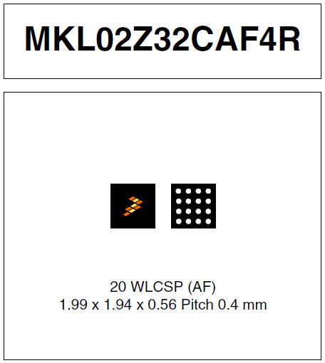
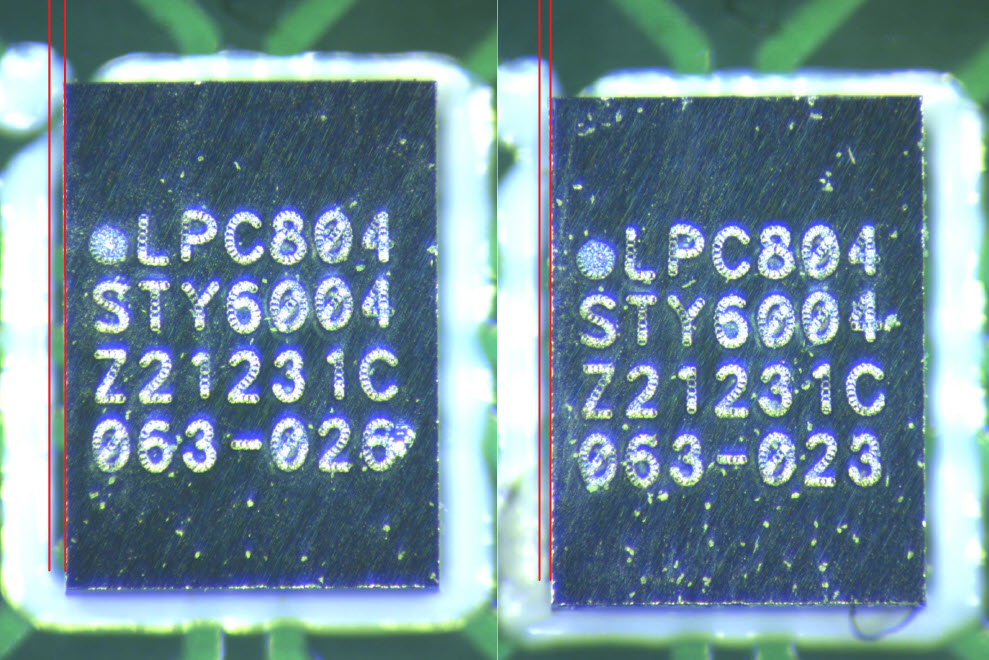
For this, two available WLCSP packages were used, both in WLCSP20: the NXP LPC804 and the NXP (Freescale) KL02Z32:
WLCSP
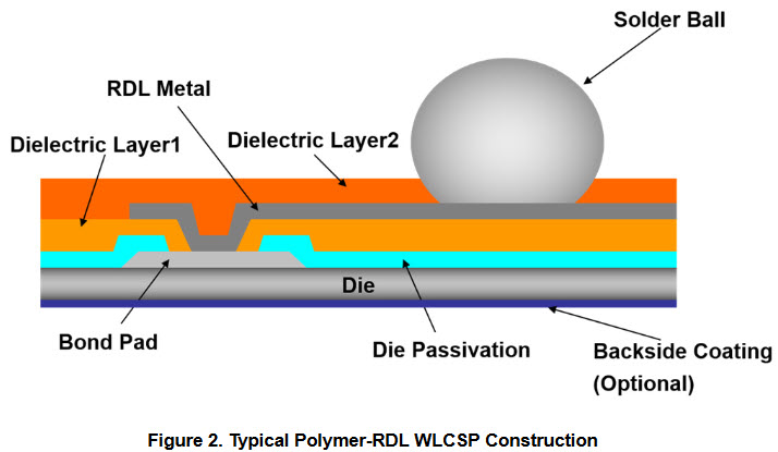
Wafer Level Chip Scale Packages are nothing new: it is a packaging technology which integrates the circuit at the wafer level, instead in a separate process with first cutting the wafer and then package it.
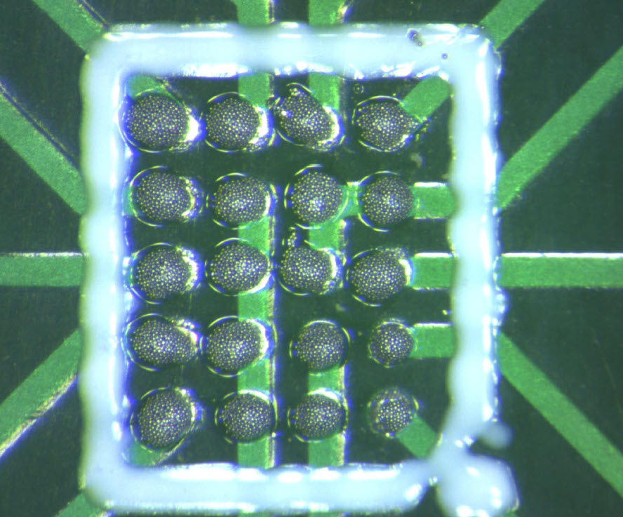
Basically it is a package directly on top of the silicon die. Or think about a ball grid package on top (or bottom) of the silicon:
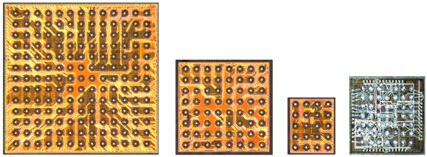
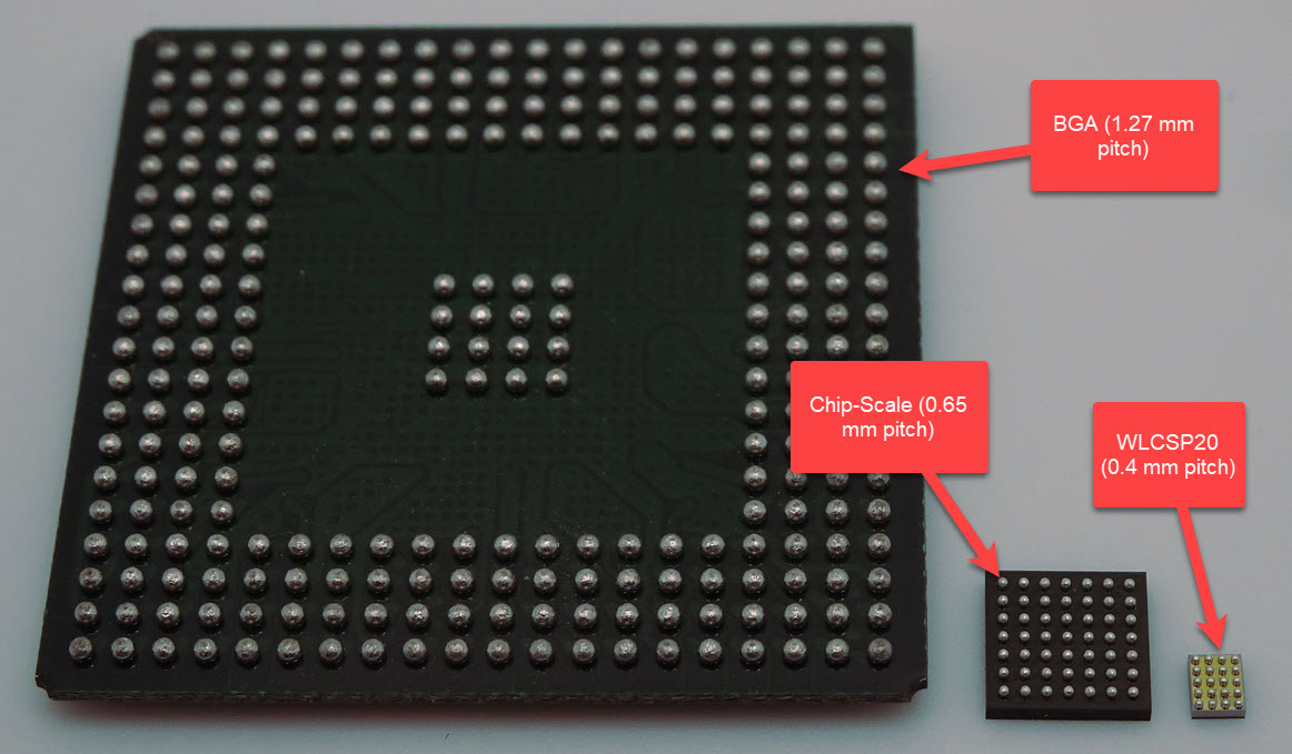
What makes it really challenging is the 0.4 or 0.5 mm ball pitch, and the routing of the signals. And WLCSC are much smaller than ‘typical’ Ball-Grid-Arrays (BGA):
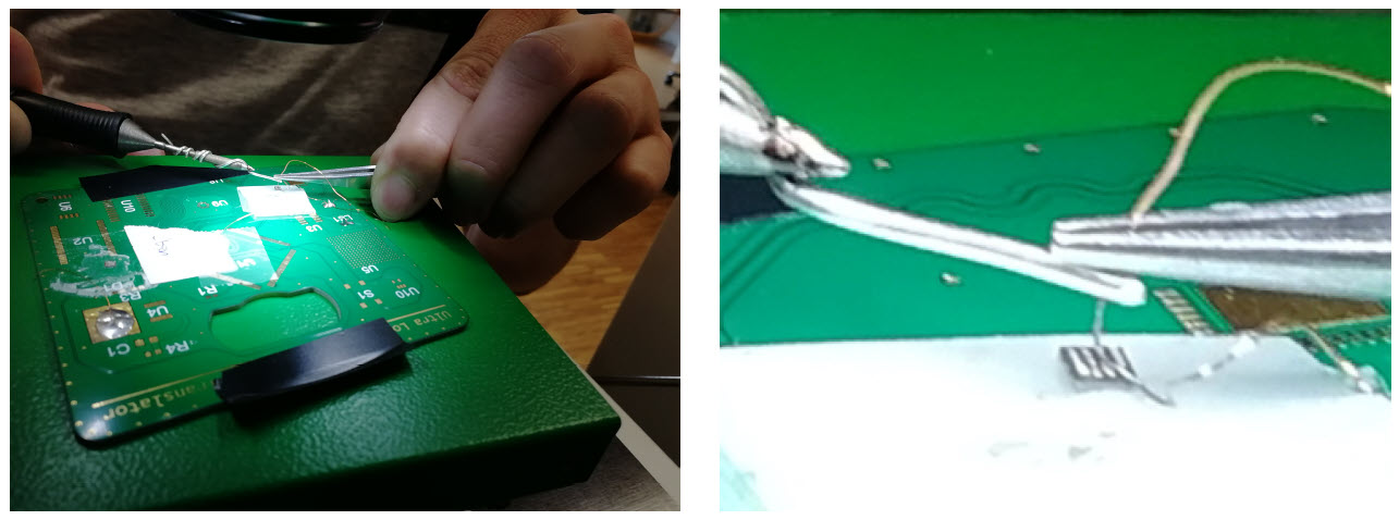
Hand Soldering?
It *is* possible to hand solder such a package, as demonstrated in a Hackaday article:

Replicating that turned out to be too difficult and failed under the microscope.
Micro-Vias
Because of the small pitch, the ‘standard’ way to deal with this is a multi-layer PCB with micro-vias, which are created with a laser.
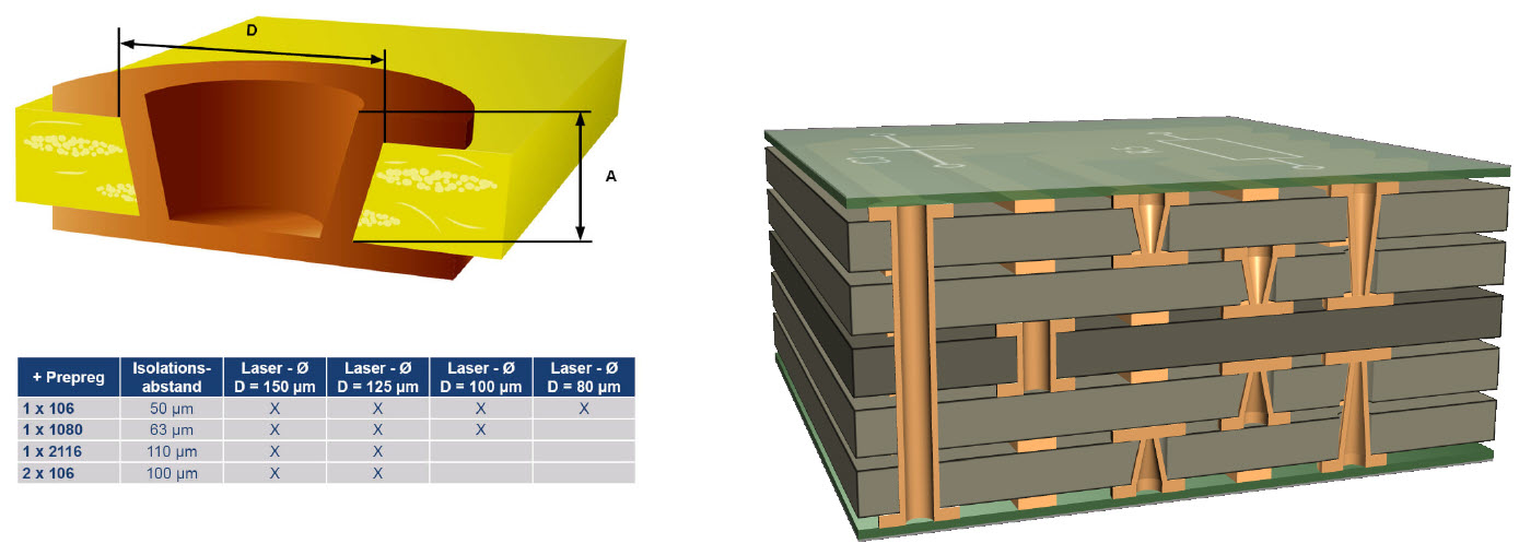
The via holes would get filled/plated for the solder ball to sit on top of it. But micro-vias and multi-layer PCBs are expensive in non-mass-volume production. So looking for alternatives.
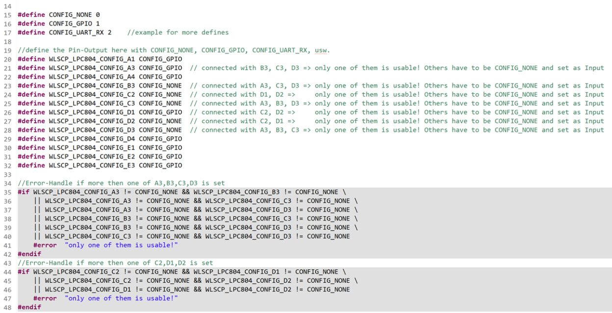
Traces between Pads
The obvious attempt would be to route the traces between the pads: The balls have a distance of 0.4 mm. The thinnest trace could be 3 mil (0.076 mm) with a spacing of 3 mil. The design rule is to have at least 0.076 mm between copper areas.
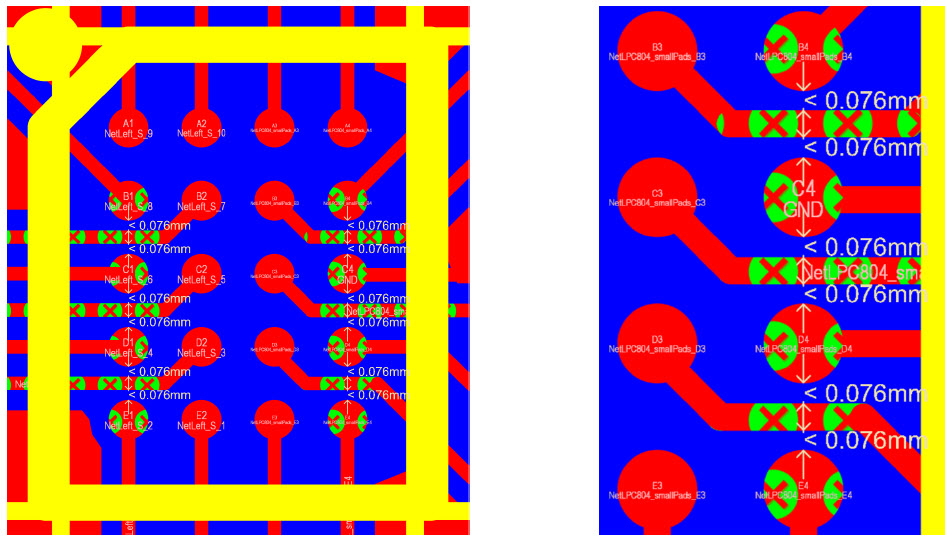
But the gaps and tolerances are to small to get this accepted with the usual manufacturing process.
Vias to Bottom
Another approach would be to place small vias and route the pins to the bottom side:
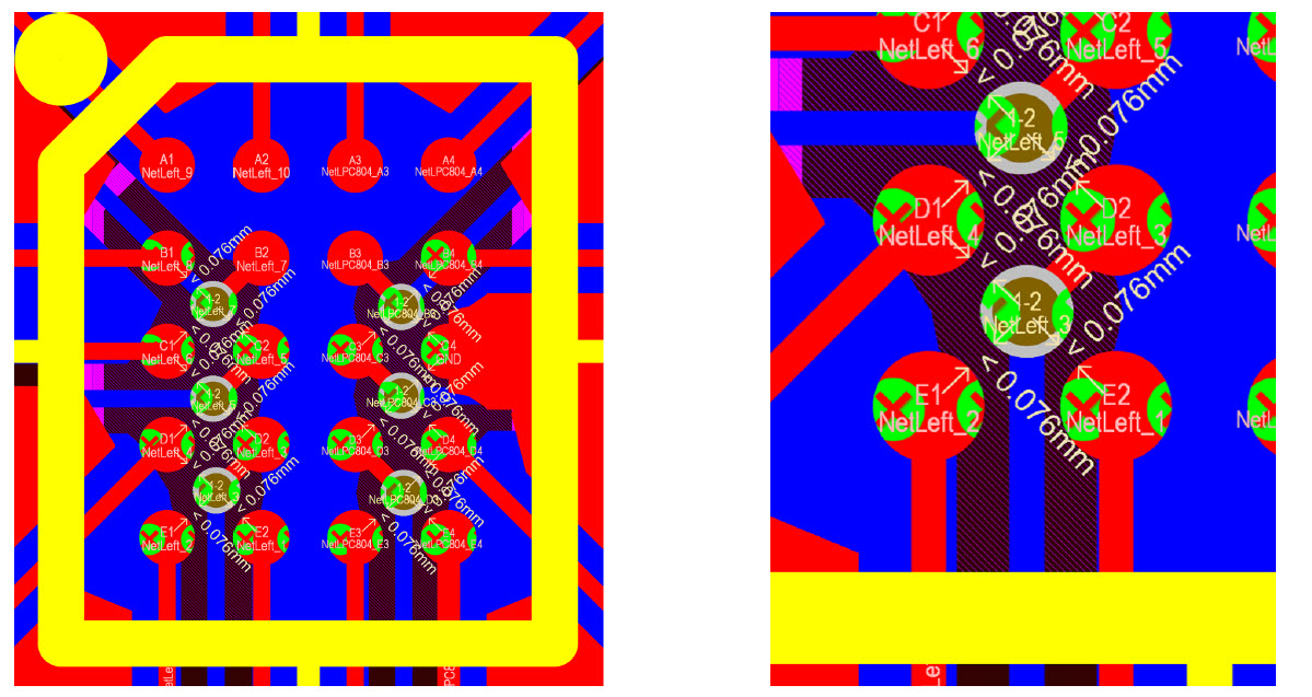
Here again, this is not feasible because the gaps are too narrow and the tolerances too high. Placing normal vias under the solder balls would suck the solder in, so this was rejected too.
Micro-Via Pads
Another idea was to use micro-vias with 0.1 mm diameter (plus 0.07 ring) inside the inner pads:
While this is technically possible, the laser can only cut thin PCB material, and production of a few PCB’s easily costs several hundreds of $. So this idea had to be stashed too, at least for now.
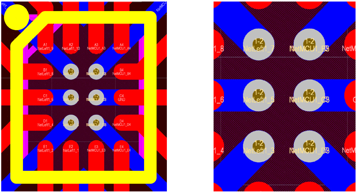
Pin Sacrificing
The last idea was to use a normal dual-layer PCB with 3/3 mil manufacturing, but sacrificing some inner pins:
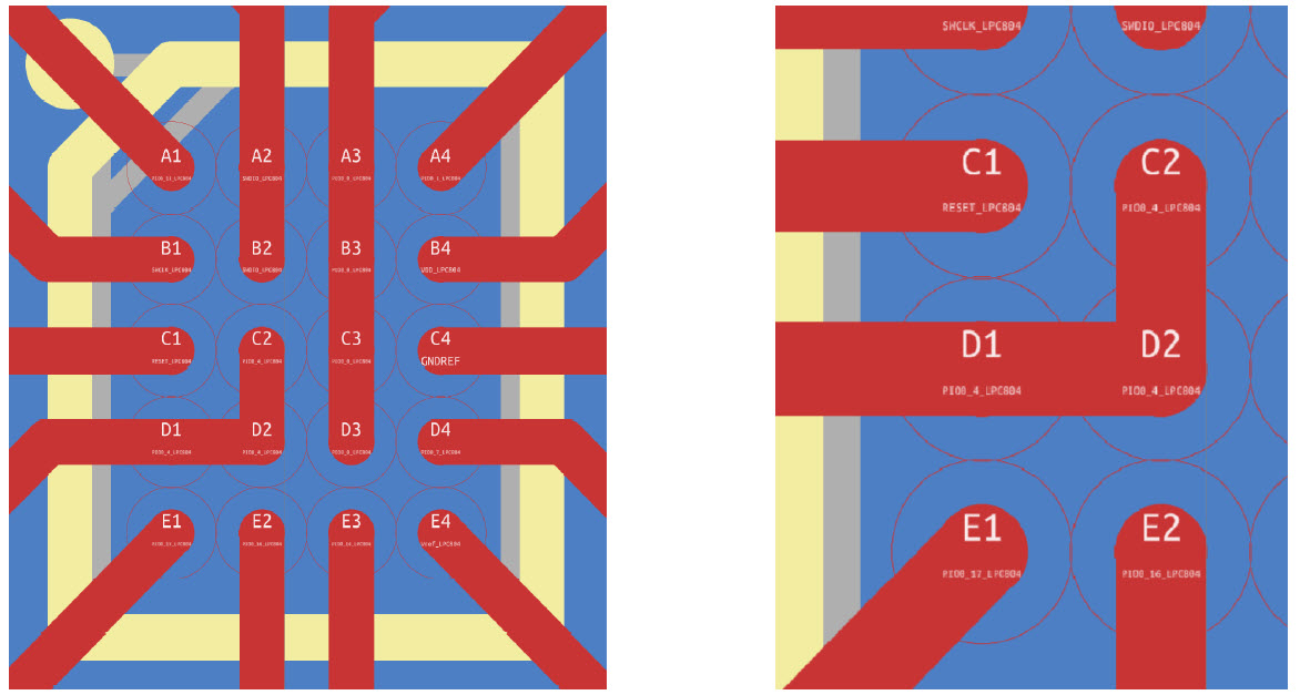
With some clever routing, it should be possible to use an inexpensive production process, while still having most of the pins and functions available. The decision has been made to try this approach.
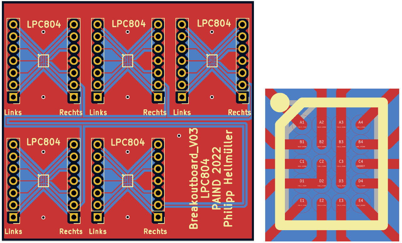
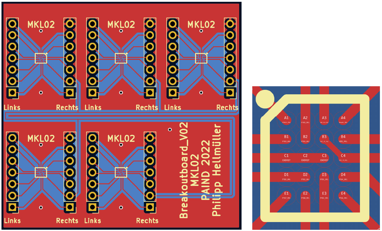
Breakout Boards
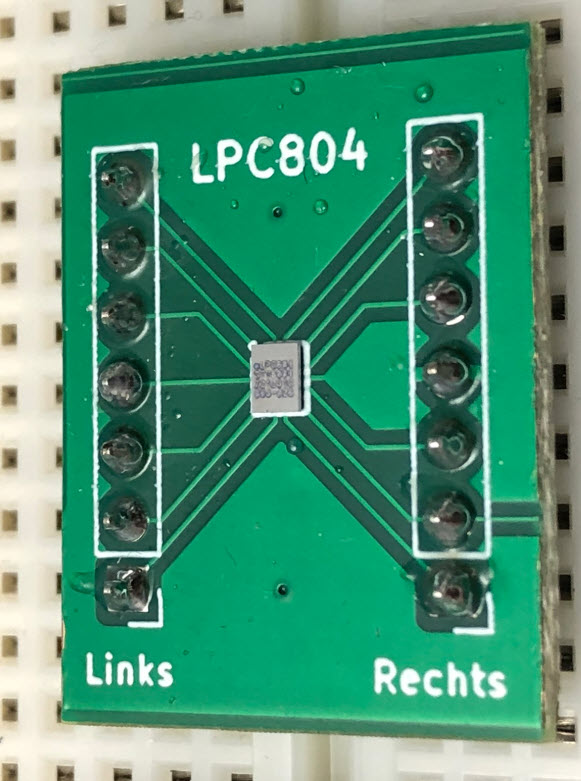
Both for the LPC804 and KL02 breakout boards have been designed:
Production of the boards worked fine. As expected, the silkscreen had some misalignment and did not help placing the MCUs:
Instead, the ‘cross-hairs’ of the PCB ‘fan-out’ traces were used to align the parts.
Solder Paste
For the first pieces, the solder paste was placed with a hand-dispenser:
Using the hand dispenser, it has been difficult to apply the right amount of solder paste, thanks to the amazing fast and steady hands of I. Habermacher!)
💡 Instead using a solder dispenser: use a stencil instead.
The MCUs then were placed by , and then put into the reflow oven.
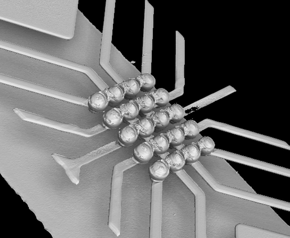
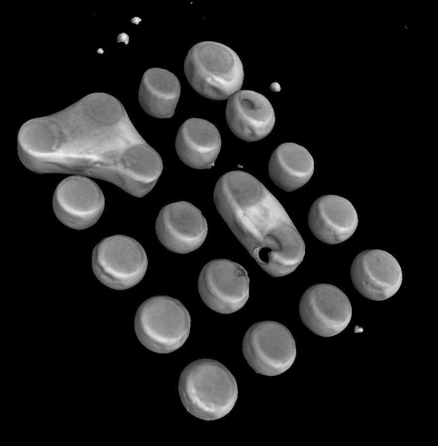
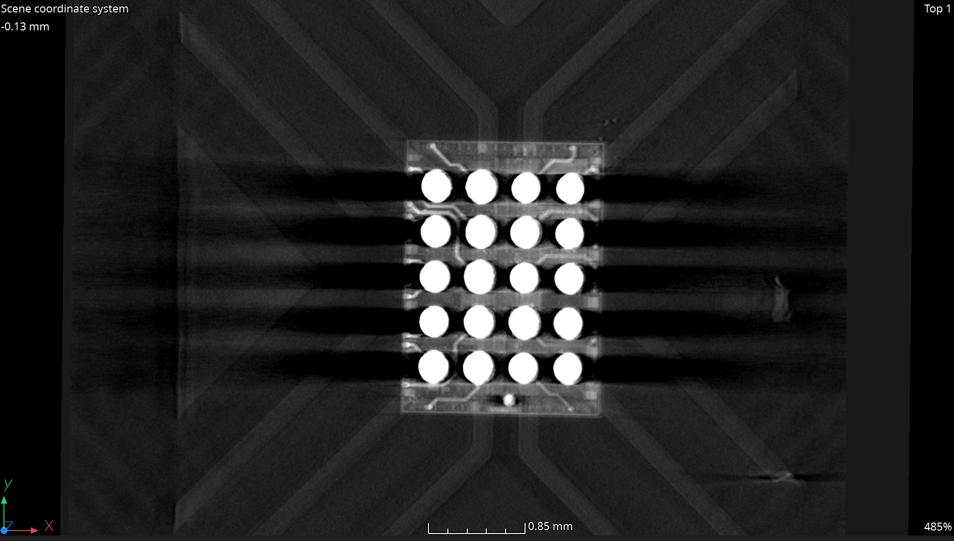
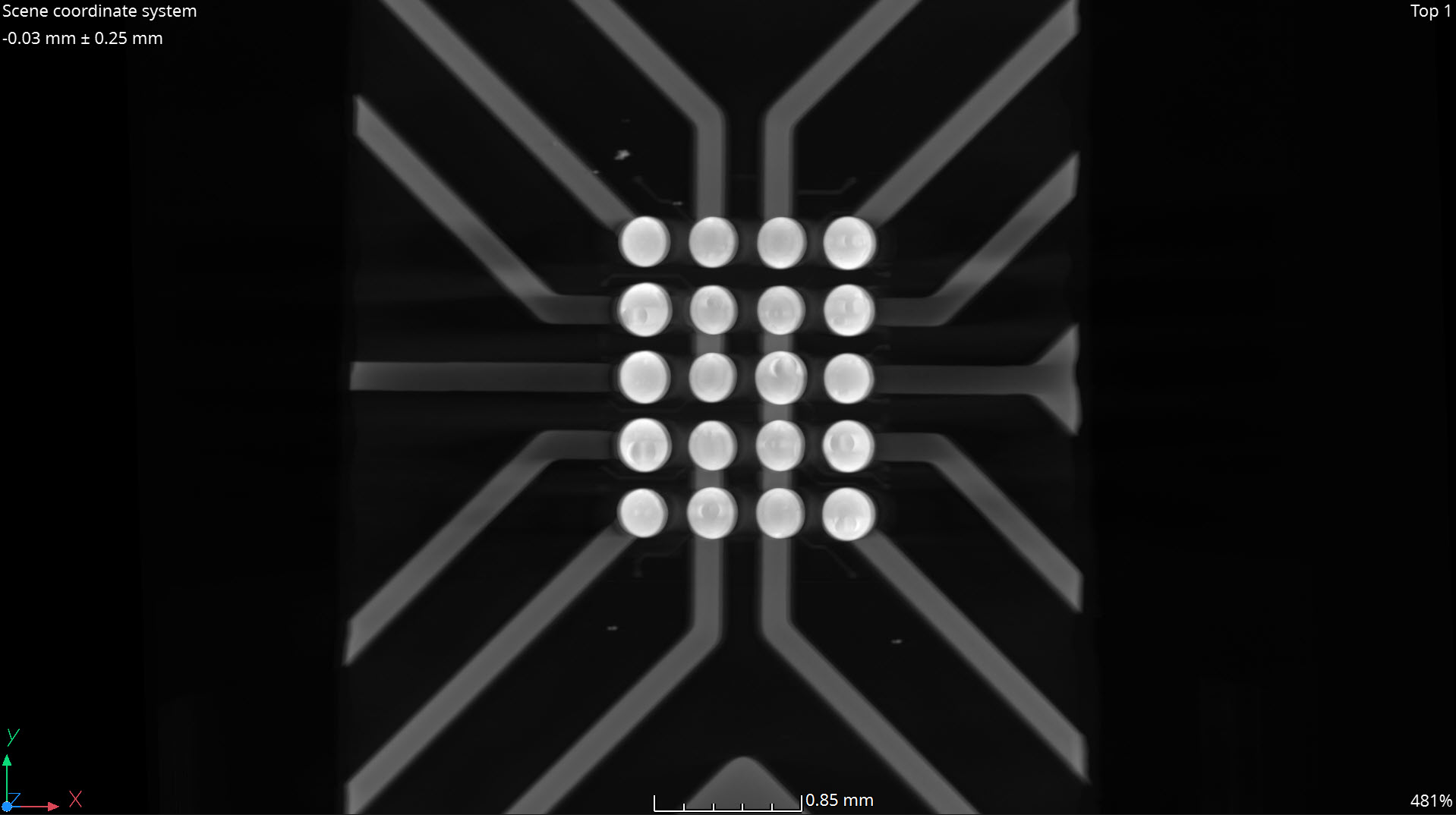
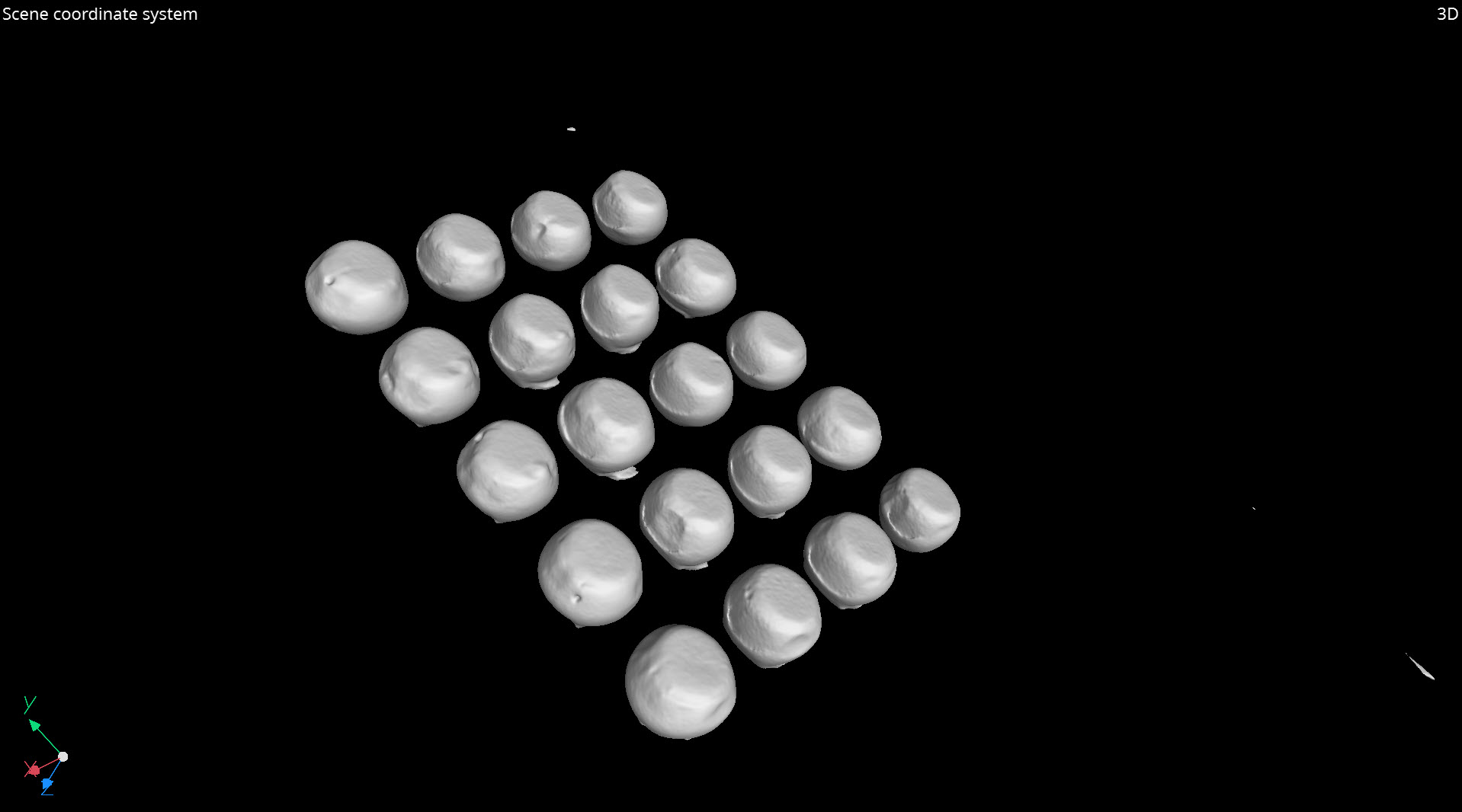
To check the amount of solder and the reflow process, the parts have been scanned with X-Rays in with ‘Luci’.
Luci
Luci is a CT (Computer Tomograph): 3.5x2x2.5 meter, around 11 metric tons. It is used for computer tomography on the campus in Horw, Lucerne.
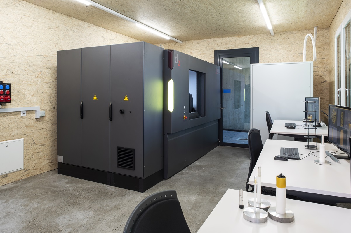
It uses X-rays and scans up to 15 images/sec, with a resolution up to 2880×2880 pixels. With Luci, different reflowed MCUs have been analyzsed.
Below is a 3D video:
The scans showed as well that in above picture with the solder paste too much was used. Plus you can see some ‘spilled’ solder balls from the reflow process.
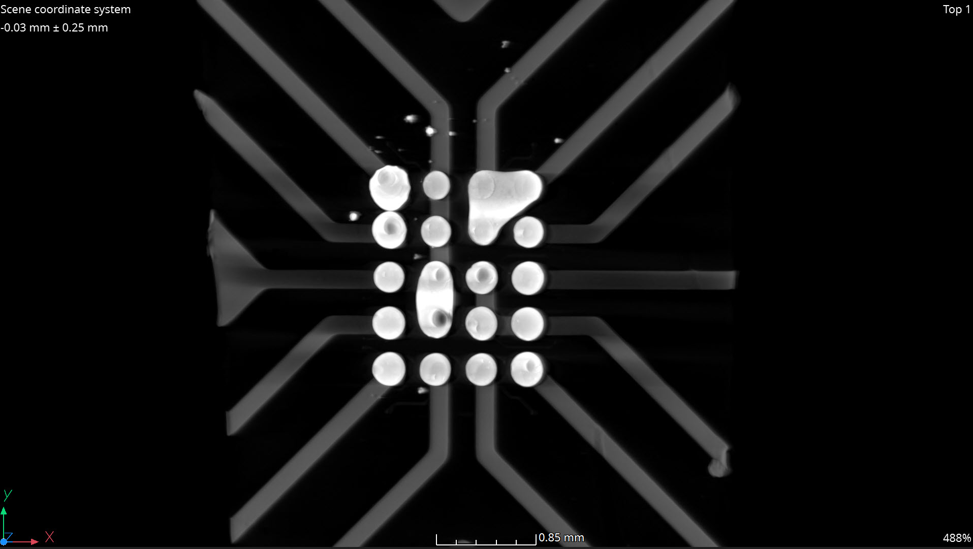
Another with less solder looked OK:
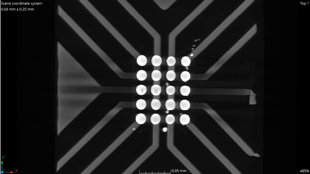
Yet another sample, this time looking perfect:
Software
To simplify pin usage and to check for not-working pin assignments, a test program with the correct pin muxing has been developed.
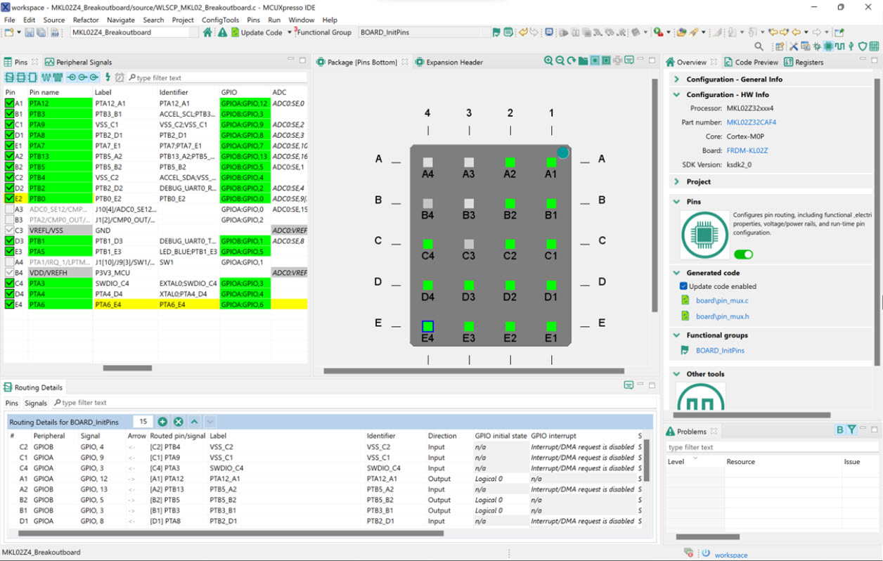
Pin assignments can be verified and checked with special assign and check macros:
Each pin and connection then has been verified, using an external debug probe:
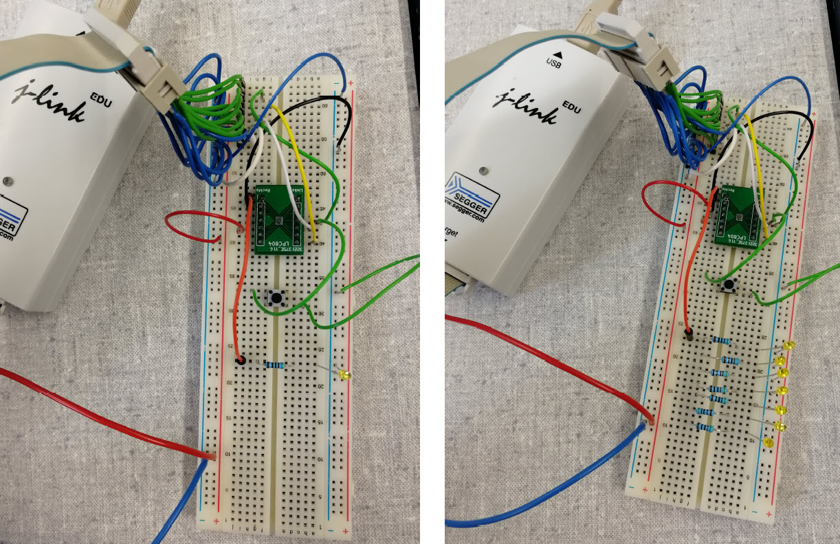
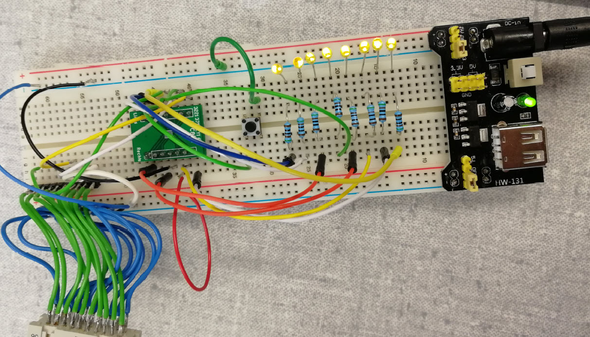
With this, the breakout boards can be successfully used :-).
Summary
It should be clear why MCUs or ICs in WLCSP packages are the last ones available on the marked. Because they are hard to use and would require complex multi-layer PCBs with expensive micro-vias. But yes, it *is* possible to use the WLCSP with some sacrifice, and they can be even soldered by hand with a reflow oven. Having a CT scanner available for sure helps to optimize the soldering and reflow process. But WLCSP are definitely not easy to use. But well, if WLCSP are the only packages you can get, then they are still in reach for smaller projects on low budget with the approach presented.
I would like to thank Philipp Hellmüller for his research, and Chris Zumbühl and Damian Gwerder for their assistance.
Happy packaging 🙂
Twist of Fate: At the end of this research project, the inventory of NXP Kinetis and LPC WLCSP MCUs at Mouser and Co. was down to zero too. I'm happy that we had received parts at the beginning, but that source for parts seems to be depleted now too, with no hope for recovery :-(.
Links
- Luci: www.hslu.ch/luci
- Luci story: https://www.hslu.ch/de-ch/hochschule-luzern/ueber-uns/medien/medienmitteilungen/2020/07/10/ein-computertomograph-fuer-die-energieforschung/
- Application note: https://www.nxp.com/docs/en/application-note/AN3846.pdf
- Hackaday article: https://hackaday.com/2022/03/21/heroic-efforts-give-smallest-arm-mcu-a-breakout-open-debugger/
- Hackaday about BGA: https://hackaday.com/2022/06/20/working-with-bgas-design-and-layout/
- Silicon Shortage and Semihosting with NXP MCUXpresso SDK on FRDM-KE02Z
- Resurrecting ‘bricked’ NXP Kinetis Devices

Fascinating, thanks! Hope we don’t hit this (our 112 pin packages would be impossible to trick, I’d guess!)
LikeLiked by 1 person
You definitely would need micro-vias for this, with increased costs for it. But for really small and tiny boards, WLCSP somewhat common. Luckily some vendors started to offer WLCSP packages with ‘gaps’ in the pin mapping, allowing to route the pins without the need for micro-vias.
LikeLike
… and you are really lucky if you are still getting MCUs these days.
LikeLike
Wow, this looks like my exact experience at work this past year. Down to the chip part# and the tried and accepted solutions. Sorry, I think it was my company that bought the remaining LPC804UKAZ on mouser/digi-key. But it got us out of a bind! (I can ask my manager if we can spare some extra for educational purposes.)
LikeLiked by 1 person
Hi Paul, so it was YOU ;-). We still have a few of these LPC804 we wanted to use for a big give-away project. Because of the part shortage, we probably have to leave the NXP land and get fully engaged in the RPi land, e.g. RP2040. ‘Forecasts’ on Mouser & Co. are +100 weeks for Kinetis, and we receive quotes on the market in the range of $150 to $600 a piece, for parts which were at $5. So my fear is that they won’t be produced any more, so time to move on ….
LikeLike
Can you share the dimensions of the pads, the solder mask opening, the stencil thickness, stencil opening, solder paste type, please?
Thank you!
LikeLiked by 1 person
See the AN3846 mentioned in the article.
LikeLike
Hi, I bought MK61FN1M0CAA12 WLCSP MCUs from rochester and got stuck with NXP SDK support. There is no SDK for MK61xx. Looking for a solution to build our prototypes, any idea how it will work if I want to use different NXP MCU?
LikeLiked by 1 person
The NXP Kinetis Design Studio with Processor Expert supports that part, so this is what I would use.
LikeLike