
Throughout this series I’ve been using the LPC55S69 microcontroller from NXP as a platform to investigate the ARM Cortex® M33 core. NXP designed the LPC55S69 with two Cortex M33 cores and so this week I’m investigating these in more detail.
You’ll remember that when ARM launch a processor core it will have a number of optional features. This is shown very clearly on the LPC55S69. The 150 MHz primary core – cpu0 – is a full implementation of Cortex® M33 and includes the optional components FPU, MPU, DSP, ITM and the TrustZone® features.

The secondary core cpu1 also operates at up to 150 MHz, however it is a more simple implementation of the Cortex® M33. In fact it does not have any of the optional features and so does NOT support TrustZone®.
In a multicore microcontroller design it is important for the two cores to have a mechanism where they can raise interrupts to the other core(s), and some form of shared memory. To maintain coherency in the shared resource it is necessary to have some form of handshaking or mutex: this will prevent both cores modifying the same data at the same time.
LPC55S69 implements those features (interrupts, mutex) in a peripheral named Inter-CPU Mailbox.
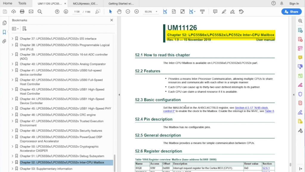
Each core can raise up to 32 interrupts on the other core, and a dedicated register – Mutual Exclusion MUTEX – contains a single bit – EX – that acts as a resource allocation handshake between the two cores. IF the bit reads ‘1’ then the core has access to a shared resource. IF the bit is high when it is read, then logic clears it to zero automatically, locking the mutex for the accessing core. The bit will automatically set high when the bit is written. If a cpu reads the bit and it is low/clear/0 then it must wait until the bit reads 1 before accessing the shared resource.
NXP have defined cpu0 as the primary core. This is the core that starts up after the chip exits from RESET. In contrast, the secondary core – cpu1 – remains in reset and does not start up until it has been configured by cpu0. The configuration includes setting up the base address in memory for the software to be executed by cpu1, and releasing it from reset.
Of course, there is a great deal of material and code examples available for the dual core implementation on LPC55S69. In this week’s video I take a quick tour of some of the documentation, and introduce the key topics. In next week’s video I’ll demonstrate how these all come together in MCUXpresso IDE when we take two of the dual-core projects for a test drive.

Pingback: Investigating ARM Cortex® M33 core – Dual Core debug tutorial | MCU on Eclipse