
To put the tinyK20 board with the NXP Kinetis K20 into bootloader mode, well someone could check the schematics, or follow this quick guide :-). In short, the pin PTB1 has to be pulled to Ground (GND) while powering the Kinetis K20. The pin PTB1 is on the outside row as below:
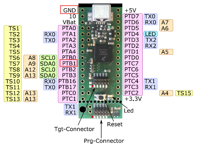
tinyK20 Bootloader Pins
GND is easy to find. The PTB1 pin is located between the 8 MHz clock and the big C near the CPU corner:
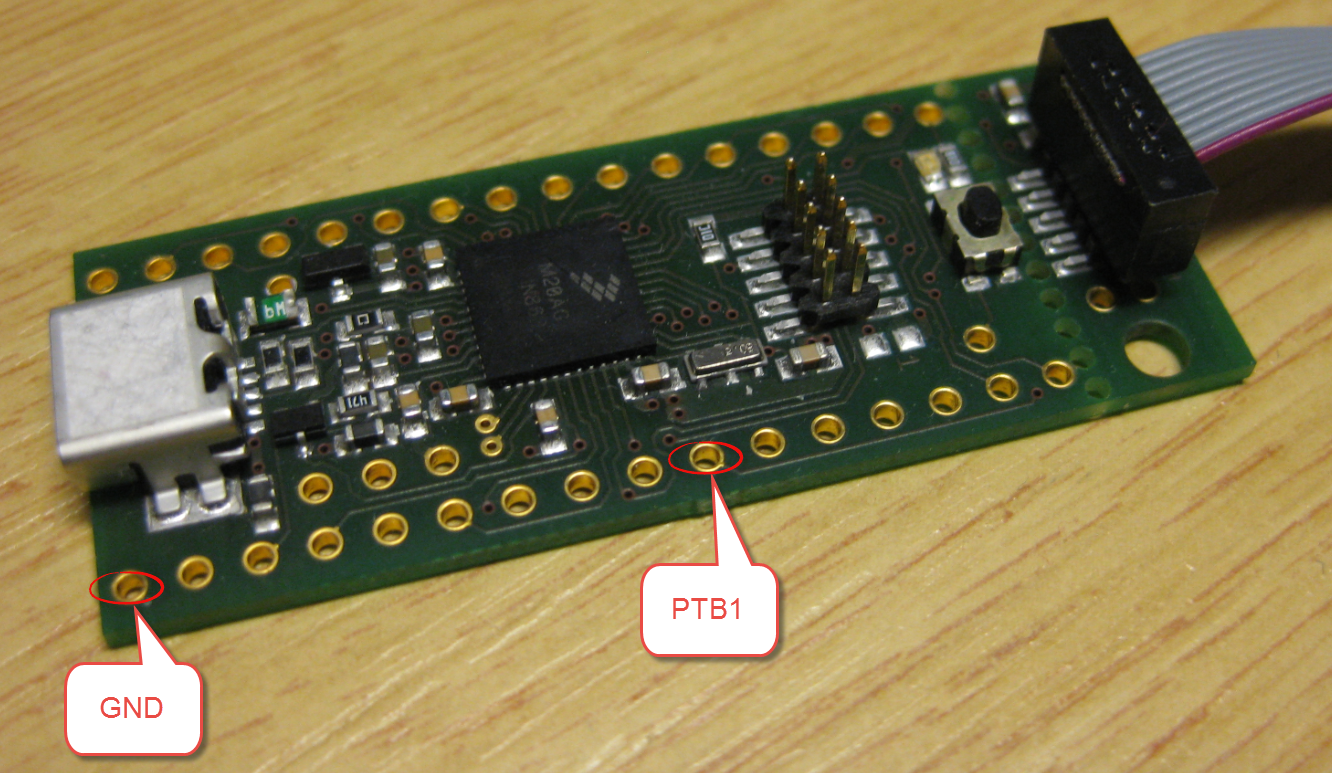
GND and PTB1 on tinyK20
I usually use a bread board wire, put into the holes, followed by powering the board with the USB connector:

tinyK20 in Bootloader Mode
Then the blue LED should start blinking and the board enumerates on the host in bootloader mode, ready to be flashed with a new firmware.
Happy Bootloading 🙂

Hi Erich,
I had a question about the OpenSDAv2 in regards how it’s used with the TinyK20. (In actuality, I have many questions posted here [https://community.nxp.com/thread/450010], but one step at a time)
Is the firmware that the TinyK20 is running capabile of not only flashing, but also debugging other targets aside from other TinyK20s? Asked another way, what limitations do I have if I wanted to use the TinyK20 as a debugger, connecting other Kinetis MCUs to the Prg-Connector pins?
Thank you!
Cruz M.
LikeLike
Hi Cruz,
it has exactly the same limitations as the OpenSDA v2 circuit say on the FRDM-K64F board. And yes, you can use it to debug other boards and use it with a debugger, with the same pros and cons as using a FRDM board for this.
On the hardware side there is just that small extension that the UART Rx/Tx pins are routed to the debug connector on the tinyK20 to allow a UART-2-USB bridge.
LikeLike
Hi Erich,
Thank you for clearing that up! Between that answer, and the reply I’ve gotten in the nxp forum, I think I have a handle on what to do.
One last thing I was curious about was why you decided to route the 10-pin header the way you did. What was the reason for putting the UART pins on pins 8/9 of the debug connector instead of 5/7 or 3/7?
To me, it seems like repurposing one of the GNDs from the connector would free up the last JTAG pin and enable the possibility of JTAG debugging.
Thanks!
Cruz M.
LikeLike
No specific reason for choosing these pins. As the OpenSDA/tinyK20 only supports SWD debugging and no JTAG, that was not something to be considered as a need.
LikeLike
Pingback: Adding a Delay to the ARM DAPLink Bootloader | MCU on Eclipse