So NXP has announced that they want to take over Freescale (see this press release). In an earlier post I experimented how Freescale tools could be used in NXP tools, see “Merging NXP LPCXpresso IDE with Freescale Kinetis Design Studio, Processor Expert and Kinetis SDK“. Just for fun, I want to do the acquisition the other way round: Using Freescale (now NXP) software and tools to build and debug the LPC824 from NXP :-).
Debugging the NXP LPC824 with Freescale based J-Link Lite
Outline
I’m using Freescale Kinetis Design Studio (Eclipse, GNU and GDB based) to create, build and debug an application for the NXP LPCXpresso824-MAX board from Embedded Artists:
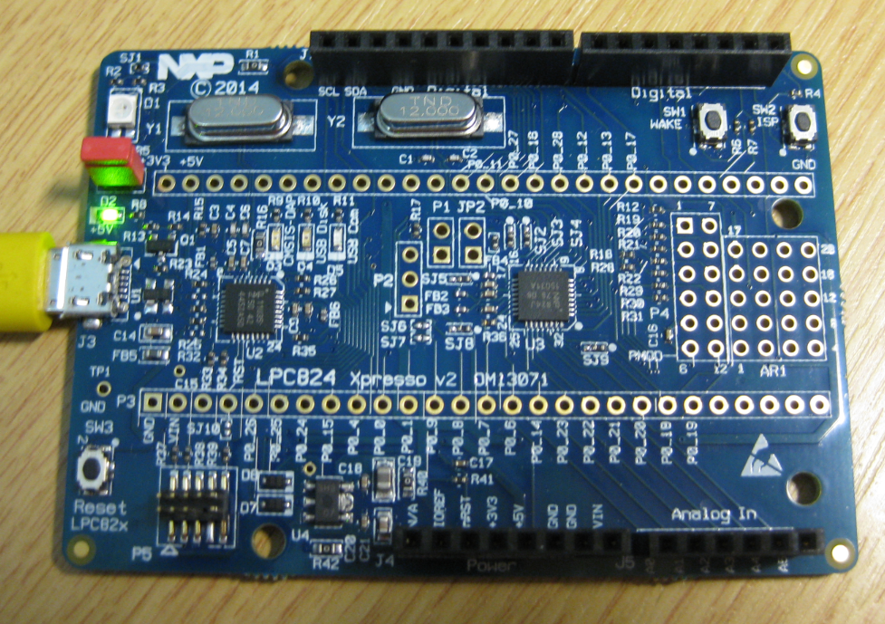
NXP LPC824 Xpresso v2 Board
The board ist the counterpart of the Freescale Freedom Boards. It has on-board (LPC-Link) debug interface. The board features Arduino Shield headers on the outside. All the processor pins of the LPC824 are available as inner rows which is really cool (I wish the Freescale FRDM boards would have that. The LPC824 (LPC824M201JHI33) on the board is an ARM Cortex-M0+ (30 MHz) with 32KByte FLASH and 8 KByte RAM. Compared to the Freescale FRDM-KL25Z (Cortex-M0+, 48 MHz, 128 KByte Flash, 16 KByte RAM, 12 CHF at Mouser.com) the LPC824 board is less powerful, but more expensive (18 CHF at Mouser.com).
Creating the Project
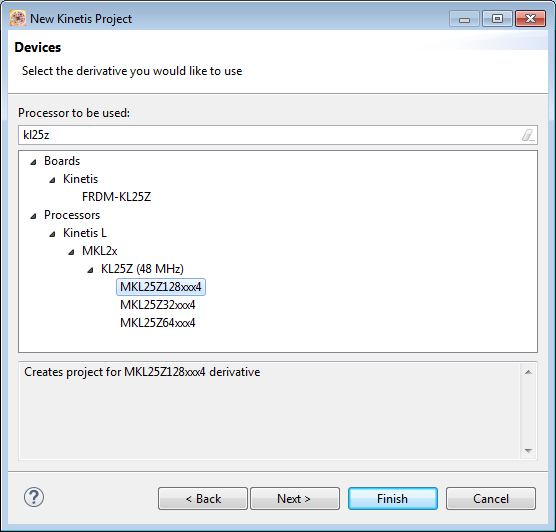
In Kinetis Design Studio, I create a project with the menu File > New. As there is (of course 😉 no NXP part listed, I select a Freescale KL25Z (ARM Cortex-M0+).
New Dummy Device Project
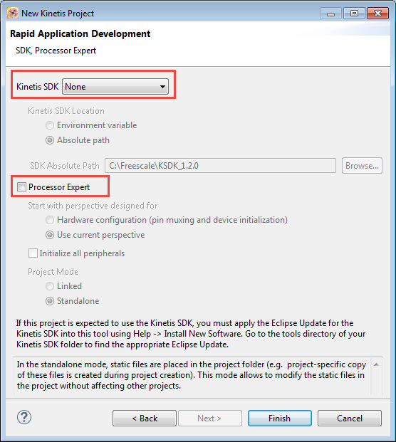
I create a ‘bare’ project (no Kinetis SDK, no Processor Expert).
New Bare Project
That project will be transformed into a project for the LPC824 in the next steps.
File Names
This step is kind of cosmetic, but will let the project look better. There are several source files in the project named after the Freescale device:
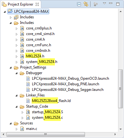
File Names
I rename them to reflect the target device:
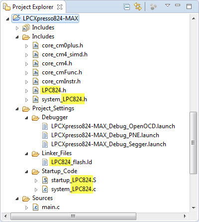
Renamed for LPC824
LPC824.h and system_LPC824.h
From LP824.h and sytem_LPC824.h I remove all the Freescale specific stuff. I’m not aiming for a full device support for now, and I can add all the LPC824 peripherals later into the header files.
System
The file ‘system_LPC824.c’ gets all the Freescale parts removed. All what remains is
#include <stdint.h> void SystemInit (void) { } void SystemCoreClockUpdate (void) { }Main
The main.c does not need to change much: only the include to “LPC824.h” needs to reflect the new device:
#include "LPC824.h" static int i = 0; int main(void) {     /* Write your code here */     /* This for loop should be replaced. By default this loop allows a single stepping. */     for (;;) {         i++;     }     /* Never leave main */     return 0; }Project Options
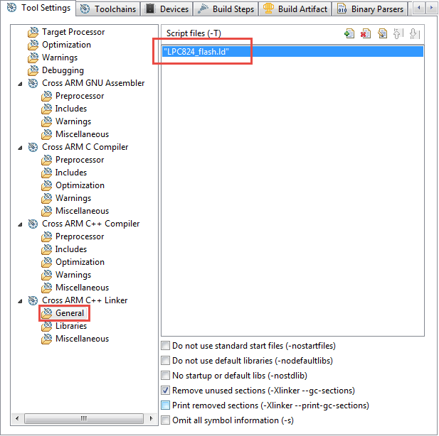
As I have changed the linker script file name, this needs to be reflected in the linker settings too:
Linker File Settings
Linker Script and Memory Map
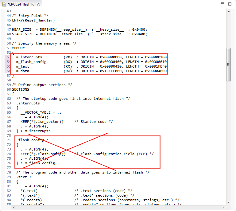
In the linker script file I need to update the memory map matching my new device, and to remove the .flash_config which is specific for the old device:
Linker Script File Changes
The memory map for the LPC824 is the following one:
MEMORY { m_interrupts (RX) : ORIGIN = 0x00000000, LENGTH = 0x000000C0 m_text (RX) : ORIGIN = 0x00000000+0xC0, LENGTH = 0x8000-0xC0 /* 32K bytes */ m_data (RW) : ORIGIN = 0x10000000, LENGTH = 0x2000 /* 8K bytes */ }Debugging
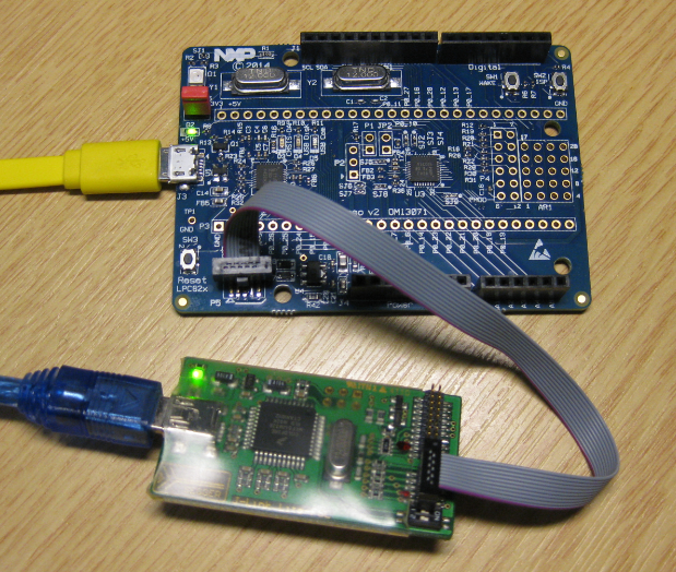
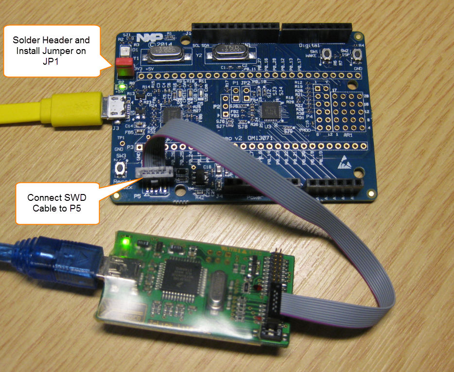
I’m using a Segger J-Link (Lite, Freescale Edition) to debug the board. To debug the board with an external JTAG/SWD adapter, I have to solder the Jumper JP1 and put a header on it. This will disable the on-chip debug device. Debugging is done through the connector on P5:
JP1 and P5 to Debug LPC82x Xpresso Board
💡 Of course I tried to debug the board using a FRDM-KL25Z (see “Debug External Processors with USBDM and Freedom Board“) as debug probe. I tried to use OpenOCD with CMSIS-DAP, but somehow the flash programming failed (wrong script file?). I tried to use the Segger J-Link OpenSDA firmware too, but this one rejected the device because it only allows to debug Freescale devices.
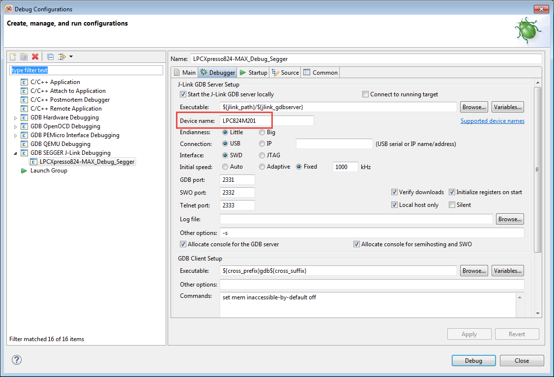
In the Segger J-Link Debugger Settings, I need to specify the correct device name: LPC824M201
Segger J-Link Device Name
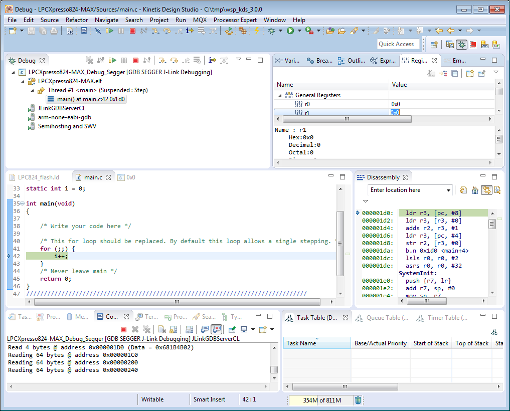
With this, I can debug the NXP LPC824 with Freescale tools: 🙂
Debugging NXP Microcontroller with Freescale Tools
Summary
It was very easy to create, build and debug a simple project for the LPC824 device from NXP, using the Freescale Kinetis Design Studio. It worked pretty out of the box with the Segger J-Link. Yes, the peripheral include files are not correctly setup, and the interrupt vector table needs to adjusted. But I can build and debug my first project on the LPC easily. So for Freescale it would be pretty easy to add NXP devices the Kinetis Design Studio (to be named differently then?). Why not combining the Kinetis SDK with the LPCOpen drivers? Why not combine the best of Kinetis Design Studio (Processor Expert! Standard GNU Tools! Segger and P&E debug connectivity!) with the best from LPCXpresso (Great wizards! Documentation! Trace!)? That would be a great combo: an Eclipse and GNU based IDE both for Freescale and NXP ARM devices :-).
The project created in this post is available on GitHub.
Happy NXPing 🙂
Links
- LPC824 Board: http://www.nxp.com/demoboard/OM13071.html
- Using Freescale Tools in NXP tools: Merging NXP LPCXpresso IDE with Freescale Kinetis Design Studio, Processor Expert and Kinetis SDK

Interesting topic. I bet you have already tried to do the same with some of ST microcontrollers…
LikeLike
Hi Marek,
the answer is: yes 🙂
Erich
LikeLike
Great:-) Maybe you could show how to deal with Discovery boards? (or Nucleo).
LikeLike
Ok, I write up an article how I use the STM32F103 Nucleo board.
LikeLike
and here we go, how to debug the Nucleo board:
https://mcuoneclipse.com/2015/08/22/debugging-stm32f103rb-nucleo-board-with-freescale-kinetis-design-studio-and-segger-j-link/
LikeLike
I have made some test and as explaned in my last reply in the link shown I think that some work has to be done by Eclipse expert.
Apart from some details the meged KDS and LPCXpresso works fine.
Pier Giovanni
LikeLike
Yes, agreed. To make them fully integrated, some engineering work needs to be done first.
LikeLike
Pingback: Debugging STM32F103RB NUCLEO Board with Freescale Kinetis Design Studio and Segger J-Link | MCU on Eclipse