
In “Eclipse MCUXpresso IDE 10.1 with integrated MCUXpresso Configuration Tools” I mentioned that I wanted to try the i.MX RT1050 processor. Well, finally my ordered board from Mouser arrived, right on time for the week-end, so I had a chance to use that ARM Cortex-M7 running at 600 MHz :-).

i.MX RT1050 EVK
💡 I highly recommend to use that board with the latest MCUXpresso IDE (currently 10.2.1) with the latest SDK.
Outline
💡 Note that in this post I have used the EVK (not the EVKB which was available later) which has the Rev A0 silicon on it. I highly recommend that you use the EVKB with the Rev A1 silicon (see errata at the end of this article).
The i.MX RT1050 is indeed an interesting device. It is an ARM Cortex-M7 running up to 600 MHz with up to 512 KByte of SRAM, but with no internal FLASH memory (‘flash-less’):

i.MX RT1050 Block Diagram (Source: NXP web site)
That device is interesting for me: image processing and number crunching demand more and more processing power and memory, and the Cortex-M4 I’m using mostly are hitting a 300 MHz ‘wall’, and the first M7 (see “First steps: ARM Cortex-M7 and FreeRTOS on NXP TWR-KV58F220M“) did not really bring the performance I hoped for. The solution I have explored so far was a combination of an Cortex-A core with a Cortex-M core (see “Tutorial: First Steps with NXP i.MX7 and Toradex Colibri Board“). But this usually requires an Embedded Linux running on the Cortex-A core: something I consider as an overkill or even a risk for running a realtime application. So that i.MX RT1050 really would close that gap and allow me continue to use the established Eclipse and JTAG debugging tools. NXP calls this device ‘crossover’ as it is bridging the gap between microcontroller and microprocessors.
What might be confusing is the ‘i.MX’ in that device name: it is not one of the traditional i.MX devices using an ARM Cortex-A: it has a single Cortex-M7 core, so it is much more a ‘normal’ Cortex-M like the ‘Kinetis’ or ‘LPC’ family from NXP, except that it seems to have inherited some of the complexity of the ‘real’ i.MX family? Anyway, as long I can use it with JTAG/SWD tools and get it run FreeRTOS, that should be fine :-).
Unboxing
I ordered my board from Mouser and it arrived after a week. The board costs around $80. It comes in a card box and with a micro USB cable which is used for power and debug.
i.MX RT1050 EVK
My board is a SCH-29538 REV A3/700-29538 REV A one. On the left above the micro-SD card socket there are headers for an Arduino shield. The device offers two micro-USB, one Ethernet port. Below a picture with the default jumper settings (click to enlarge):
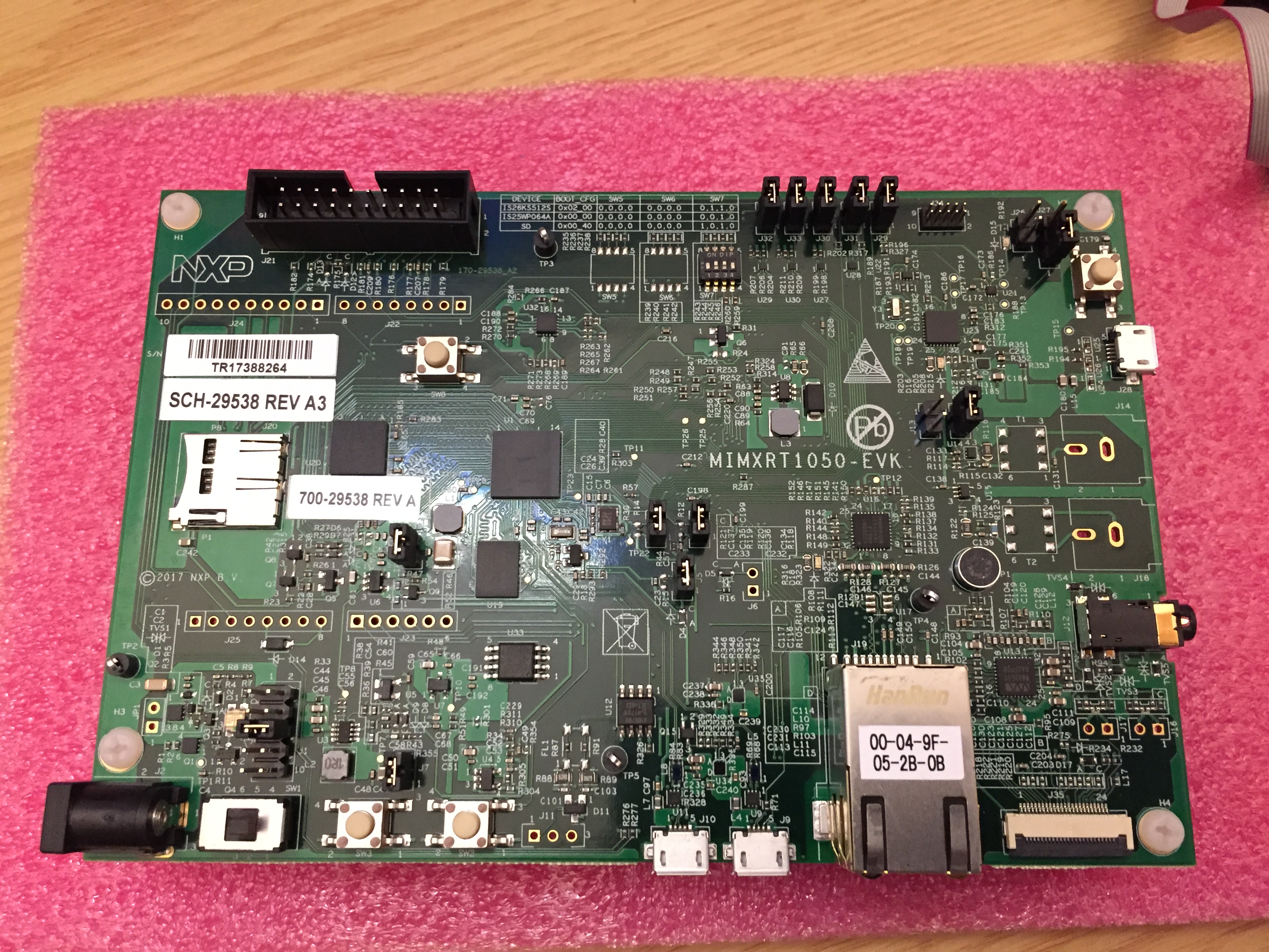
MIMXRT1050-EVK
On the backside there are connectors for a display (left connector) and a touch interface (right connector). I guess I will try to order the matching display from Mouser too.
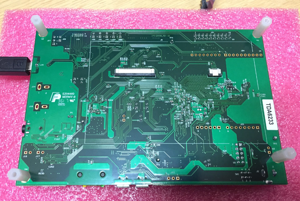
i.MX RT Board Bottom Side
The device of interest on the board is the MIMXRT1052:

i.MX RT1052 Device
Power
The board can be powered through the Debug (DAPLink/OpenSDA) USB port:

Power with DAPLink Port
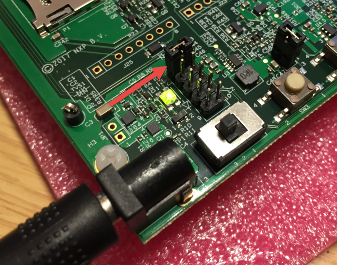
In that case, jumper J1 near the power LED should set to the *middle* position:
DAPLink Power Option
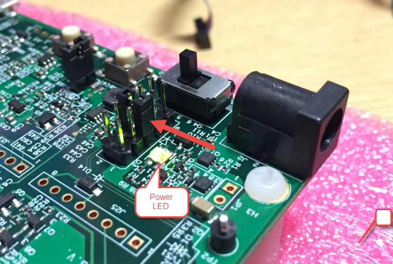
I prefer to use an external power supply, as I have faced issues with other boards if they draw too much power (and some forum posts indicate some potential USB power supply issues too). Using an external power supply I can use the ON/OFF switch near the barrel connector. The board needs a 5V DC Power supply (Center +5V, outside GND). If using an external power source, the Jumper on J1 has to be set to the *top* position:
External Power Connector
The green LED shown in above image indicates that the board has power. More than once it happened I failed to debug the board because it was not powered :-(.
Boot Options
The board can boot up from different memory using the boot option switch SW7:

SW7 Boot Options
I’m using the default option to boot from ‘Hyperflash’ with the following settings
SW7: 1-OFF 2-ON 3-ON 4-OFF
Memory
In ‘normal’ microcontroller, there is SRAM and FLASH available out of reset. As this device is ‘flash-less’ at boot time, the memory management and configuration is a bit more challenging.
The RT1052 has 512KB RAM on-chip, available at boot time. It is splitted up into SRAM_OC (On-Chip), SRAM_ITC (Instruction-Tightly-Coupled) and SRAM_DTC (Data-Tightly-Coupled). Below they are shown in the Memory configuration editor inside the MCUXpresso IDE:
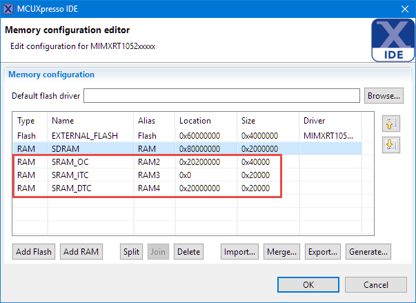
RT1052 Memory Map with on-chip RAM
The 128 KByte ‘ITC’ RAM is optimized for instruction execution, while the 128 KByte ‘DTC’ RAM is optimized for data access.
External to the RT1052 there are 4 extra memory options:
- 64 MByte ‘Hyper Flash’
- 32 MByte SDRAM
- 8 MByte QSPI Flash
- micro SD card socket

RT1052 with external Memory Devices
Both the external Flash (‘Hyperflash’) and SDRAM are not available right away at boot time. The bootROM will check the external Flash for a specific header: if this header is found and valid, the Flash can be used and it will use that information to initialize the external SDRAM too. Presence of that header is critical, as it allows executing code from that external FLASH memory, also called XIP (eXecute In Place).
Below the 512MBit/64MByte ‘Hyper Flash’ from Spansion and the 8 MByte QSPI on the right:
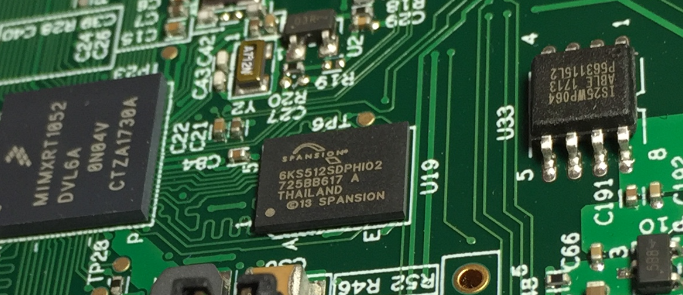
Spansion Flash Device plus SPI Flash
The 32 MByte 166 MHz SDRAM device:

SDRAM
The 8 MByte QSPI Flash device:

QSPI 64MBit FLASH
It looks like the QSPI Flash is not really usable. From the user manual:
“By default, this QSPI Flash is disabled on the EVK. To enable it, Hyper Flash should be removed when the QSPI Flash is selected as the boot device. And R153, R154, R155, R156, R157, R158 should add 0 Ohm resistors.”
Does this really mean *removing* the Hyper Flash device from the board?
On-Board Debug Interface
The board features includes the DAPLink (or OpenSDA) on-board debug interface as present on many other Freescale/NXP boards.
The programmed DAPLink firmware information is
# DAPLink Firmware - see https://mbed.com/daplink
Unique ID: 0225000041114e4500463009c207001792d1000097969900
HIC ID: 97969900
Auto Reset: 0
Automation allowed: 0
Daplink Mode: Interface
Interface Version: 0241
Bootloader Version: 0242
Git SHA: 34182e2cce4ca99073443ef29fbcfaab9e18caec
Local Mods: 1
USB Interfaces: MSD, CDC, HID
Bootloader CRC: 0x73707d49
Interface CRC: 0x92919274
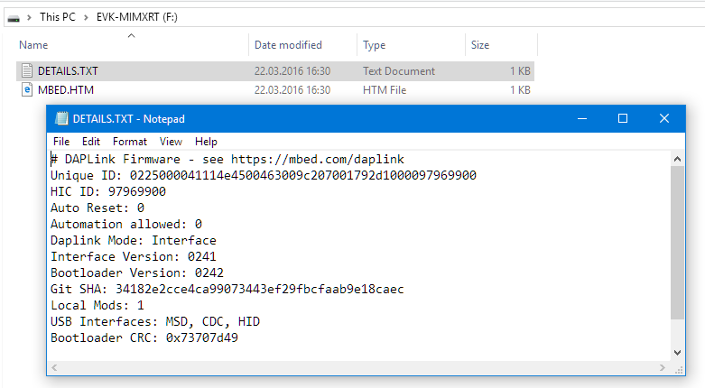
DAPLink Firmware
Because that firmware is not the latest one, I downloaded the latest one from http://www.nxp.com/opensda. The same link is available in the MCUXpresso IDE:

OpenSDA Firmware Update Site
There are two different firmware binaries for debugging with CMSIS-DAP: one for SPI-Flash and one for Hyper-Flash.
💡 I have only used the Hyperflash one. I could be that the difference is where the USB MSD flashloader stores the binary. Anyway I’m not using that loader and using the debugger instead.
Because the board is initially configured to use Hyperflash, I have downloaded that firmware (I downloaded both, just in case, but make sure you use the correct one depending on your flash configuration):
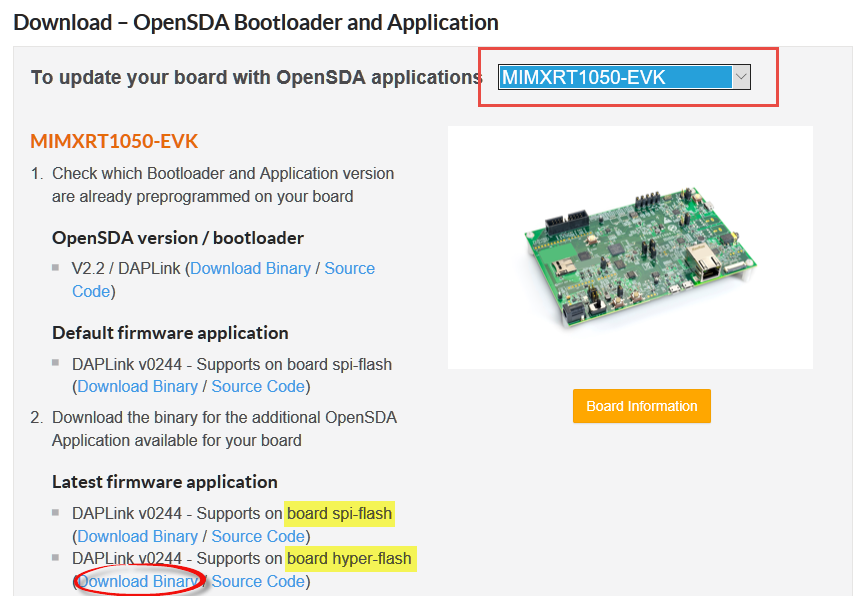
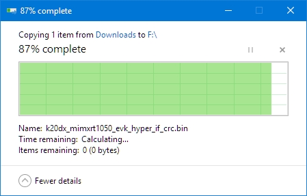
Download OpenSDA Binary
This downloads k20dx_mimxrt1050_evk_hyper_if_crc.bin for me.
To program the new CMSIS-DAP firmware:
- Power off the board
- Make sure Jumper J27 is on 1-2 position:

Jumper J27 in 1-2 position
- Press and hold SW4 while powering the board, then release SW4
- The device should show up as ‘MAINTENANCE

DAPLink Maintenance Mode
- Copy the .bin firmware file downloaded to that drive/device (e.g. drag&drop)

Downloading DAPLink firmware
- Power off the board and power it again. Check the Interface Version (this is the new CMSIS-DAP Firmware version):

Updated CMSIS-DAP Debug Firmware
- Power off the board again. Set Jumper J27 to the position 2-3 for OpenSDA Debug
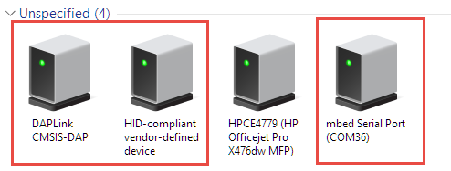
- Power on the board again. On Windows, under Devices/Printers it should show now three additional devices:

DAPLink CMSIS-DAP Devices
- Now we are ready to debug it :-).


MCUXpresso SDK
The SDK (software drivers) for the device are availble from http://mcuxpresso.nxp.com/. After selecting the device I can build the SDK:

MCUXpresso SDK Page
This gives me another page of options for the SDK. Make sure to select the MCUXpresso IDE. With the ‘Add software component’ I can add extra components as FreeRTOS. Then download the SDK.

Configured the SDK
MCUXpresso IDE
I’m using the MCUXpresso IDE V10.1.0 (see “Eclipse MCUXpresso IDE 10.1 with integrated MCUXpresso Configuration Tools“). The downloaded SDK from the previous step gets added with drag&drop into the ‘Installed SDK” view:

Installed SDK in MCUXpresso IDE
Create a new project with the shortcut in the Quickstart Panel:
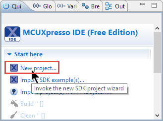
Creating New Project
Select the board, then press next:

Creating Project for 1050
In the next page I have selected FreeRTOS (or go with the defaults):

Configure the Project
Pressing next gives the advanced options which I keep at the defaults:
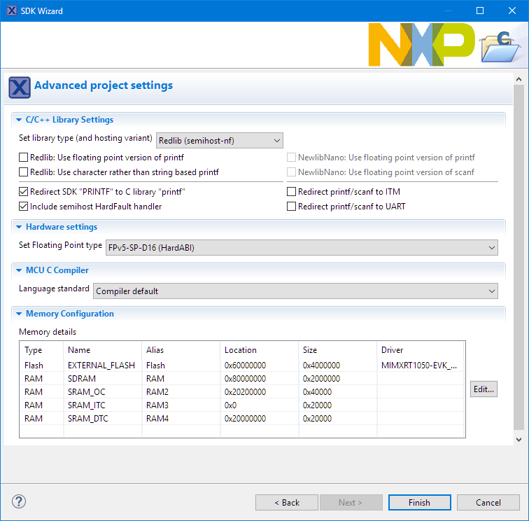
Advanced Project Options
With ‘Finish’ the project gets created, and I can build it:

Building project
Debug
💡 My board had problems with debug, because probably the content of the external FLASH block confused the bootROM, so debugging was not possible. Consult the ‘Troubleshooting’ section at the end of this article for erasing the external FLASH first.
To debug the project, use the ‘Debug’ button from the Quickstart Panel:
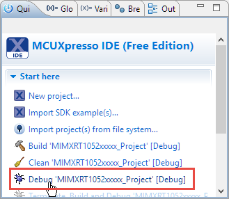
Debug from the Quickstart Panel
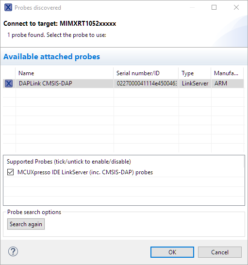
The first time, it will trigger a probe discovery, and the DAPLink probe should show up:

Probe Discovered
With this can debug that ‘hello world’ project in the MCUXpresso IDE:

Debugging Hello World
Execute in Place (XIP) Header
As seen from the Disassembly view above, the program is executing from the external FLASH at 0x6000’0000 :-). The project has files in the ‘xip’ folder to create and link the needed header at address 0x6000’0000:

XIP File in Project
This creates a 8 KByte special header at the beginning of the the FLASH at address 0x6000’0000:

Hyperflash Config Block
Most of the SDK examples are running in RAM. To change them to run from the external FLASH, consult the Overview Guide.
Debug Connector J21
If using an external SWD/JTAG debug probe, the board has a connector for the main CPU located on J21. In the picture below I have attached the NXP LPC-Link2 probe with a custom enclosure (see “Custom 3D Printed Enclosure for NXP LPC-Link2 Debug Probes“).
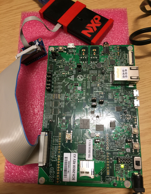
LPC-Link2 External Debug Probe
Debug connection with the P&E Multilink Universal:
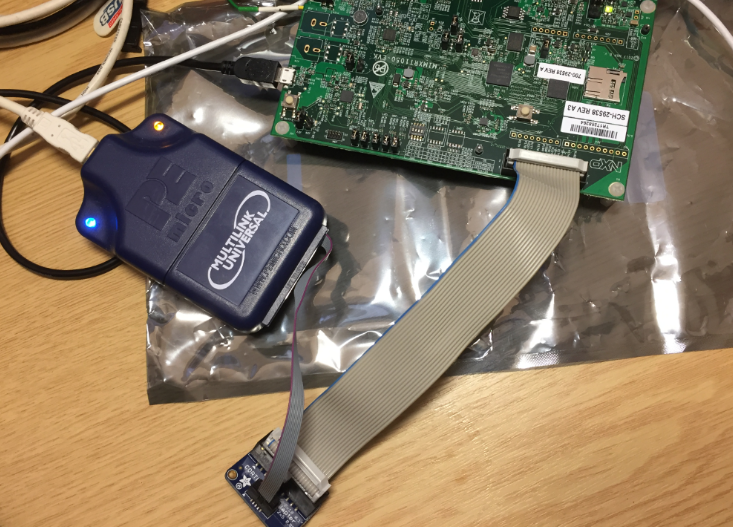
Debugging with P&E Multilink
Same with the Segger J-Link:

Debugging with J-Link
There are two jumpers to disconnect the JTAG signals. While it *might* work with the jumpers installed, I highly recommend to remove the jumpers J32 (SWD_DIO_TGTMCU_BUF) and J33 (SWD_DIO_TGTMCU_BUF) if using an external debug probe:

J32 and J33 removed for external debug probe
The onboard DAPLink debugger is not that fast. What helps for the LinkServer/OpenSDA debug connection is to remove the following (see Overview Guide):
--cachelib libm7_cache.so

removing cachelib libm7_cache.so
That removes the extra cache handling, making debugging about twice as fast. Speed is ok that way, but not at par use an external debug probe. If you are really serious about debugging, get an external debug probe.
For using it with a small 2×5 0.05″ cable, I have to use an adapter board, e.g. the one from Adafruit.
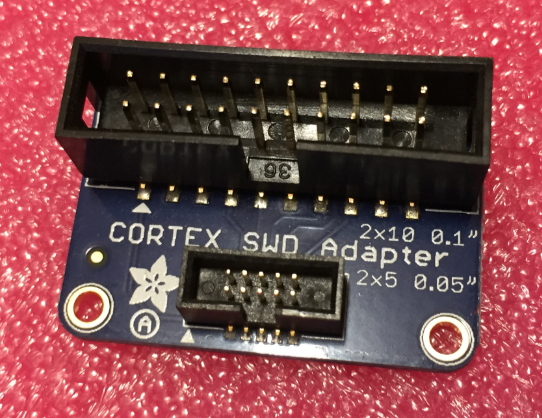
Cortex SWD Adapter
I have been able to use onboard DAPLink, Segger J-Link, P&E Multilink and the NXP LPC-Link2 to debug the board.
Trouble Shooting
I was not able to debug my board, probably because the bootROM was confused by some wrong values in the external Hyperflash at address 0x6000’0000. To solve that problem, erase the FLASH memory. With the MCUXpresso IDE, either the onBoard DAPLink with CMSIS-DAP or the NXP LPC-Link2 Debug probe on connector J21 has to be used (the P&E or Segger probes won’t help here).
First, power off the board and change the SW7 DIP Switch to
SW7: 1-ON 2-ON 3-ON 4-OFF
to prevent booting from Hyperflash:

Preventing booting from Flash
Power the board again. Select a project setup for XIP, and start the GUI Flash Programmer in the MCUXpresso IDE:
GUI Flash Programmer Icon
The project must have a DAPLink or LPC-Link2 debug connection:
DAPLink Connection
Next, make sure that the ‘Mass erase’ option is enabled:
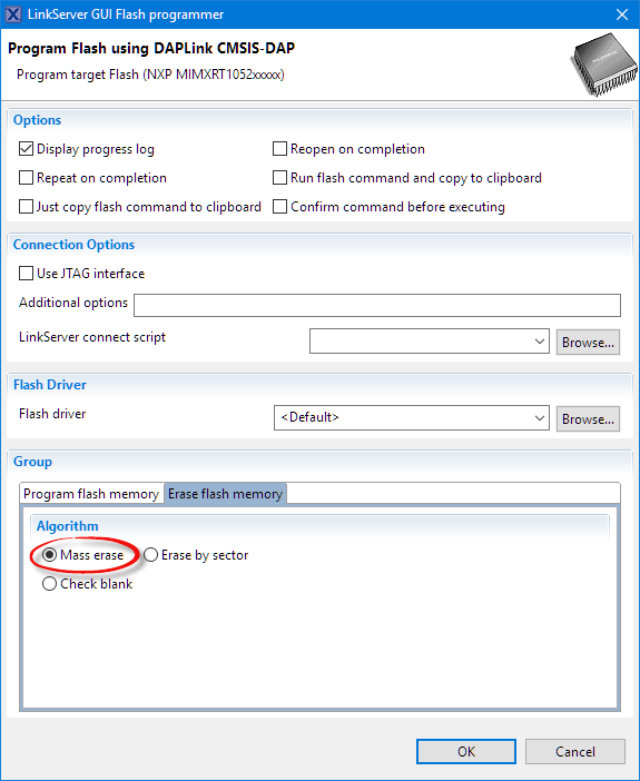
Mass Erasing Device
Press OK:

Mass Erase Progress
This will trigger the following dialog which can be closed:
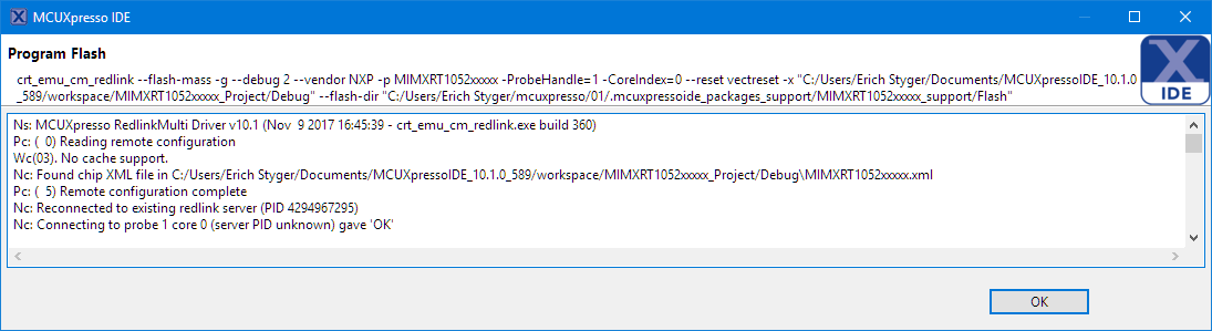
Program Flash
Power off the board, restore the SW7 to the allow boot from Hyperflash again:

Boot from Hyperflash
Because the Hyperflash boot block is now erased, the board should be useable again.
Summary
The i.MX RT1052 is indeed an interesting device: lots of performance. According to NXP Factsheet the price should be reasonable too: “10k resale at sub $2.50”. Still there will be costs at least for an external FLASH memory. That BGA package makes it tricky for hobbyist. Usinig the MCUXpresso IDE makes it a very good experience to make the first steps with that board. While the onboard DAPLink is convenient, I recommend using an external debug probe. Finally, maybe board vendors will come up with small and bread board friendly breakout boards for the i.MX RT?. Something like the tinyk22? That would be awesome!
Happy RT’ing 🙂
Links
- NXP i.MX RT Web Page: https://www.nxp.com/products/processors-and-microcontrollers/applications-processors/i.mx-applications-processors/i.mx-rt-series:IMX-RT-SERIES
- Overview of using the MIMXRT1050-EVK with MCUXpresso IDE: https://community.nxp.com/community/mcuxpresso/mcuxpresso-ide/blog/2017/12/07/overview-of-using-the-mimxrt1050-evk-with-mcuxpresso-ide
- MCUXpresso IDE: http://www.nxp.com/mcuxpresso/ide
- MCUXpresso SDK: http://mcuxpresso.nxp.com/
- Difference A0 and A1 silicon: https://www.nxp.com/docs/en/nxp/application-notes/AN12146.pdf
- i.MX RT1050 EVK(B) guide: https://www.nxp.com/docs/en/user-guide/MIMXRT1050EVKHUG.pdf
- Using QSPI instead of Hyperflash (SEGGER): https://wiki.segger.com/IMXRT105x

Thanks Erich – Can you comment on the performance trade-offs for executing from different kinds of external flash vs. code copied into internal RAM?
LikeLike
Hi Dave,
I have not reached that point yet. The ‘tightly’ coupled memory is not cached. I was considering toggling a pin with code running in the different areas.
LikeLike
It always interesting to see a new line of MCU. In this case the devices have the potential to provide an upgrade path to the devices I have been using with the added bonus of not having to become familiar with yet another IDE and SDK. Having recently looked at options for an upgrade path in the context of new requirements, it has become clear that what would really speed up development of solutions and make these boards competitive with the population of Raspberry PIs out there would be a greater focus on application and operating system level software that is required for many applications such as reliable USB Mass storage file system, FTP, shell script capability and so on whilst still maintaining Micro controller real time capability. The Middle-ware from Arm seems to fill that gap and MDK5 supports this i.MX RT line already.
LikeLike
I think these days it is more about the software and tools than about the hardware itself. Yes, the hardware is needed, but my key decision factor for a design is the availability and quality of the software and tools, and this includes the middleware and drivers. The Raspy is a good example: that hardware is not really great or best in class, but the available tutorials, courses, middleware, etc are.
LikeLike
Hi Erich,
After re-discovery the debugger probe, it can work .
Thanks a lot,
Best Regards,
Kent
LikeLike
Hi Erich,
I’ve one of this 1052 EVK boards and a Jlink probe ..
Just a small curiosity : why do u need two adapters to connect to the JTAG connector ( J21 ) ?
I would not be more “straight” to go directly from the 20 pin 0.1 mm connector on the JLink to the 20 pin 0.1 mm on the EVK board ?
From the EVK schematich and JLink connector footprint seems there should be no problems …
LikeLike
Yes, I can go straight with the ‘big’ cable from the J-Link to the board, that’s correct. I’m usinig the adapter with the small cable for convenience only (easier to move around the probe, as my desk gets messy 😉
LikeLike
Hi Erich,
I m trying to use Jlink with Mcuxpresso but failed. the error message is “cannot get jtag device”. is there any special configuration settings for Jlink debugger?
Thanks a lot.
Best Regards,
Kent
LikeLike
Hi Kent,
no, no special setup or settings are needed. Have you created a project with the wizard (File > New) inside MCUXpresso using the SDK project? This should setup your connection when you do a debug the first time.
LikeLike
Many thanks for the clarification !
Luca
LikeLike
Hi! In my view this board have a nice MCU and stuff on it! But it have a really bad layout! It only have arduino headers as “easy” expansion ports the other ones are only fpc conectors! In my opinon it’s better to wait for a board with more pins exposed! For 80$ it’s quite expensive!
LikeLike
Mat,
Embedded Artists has a SODIMM module with this CPU on it – don’t know the price, but I would expect it to still be higher than you like. These are Eval boards, and are priced as such. Once you embed the CPU on your own hardware the costs will come way down.
Brynn
LikeLike
I attended a webinar by Embedded Artists, and there I saw that module. But I have not seen it for sale somewhere. My understanding is that Embedded Artists makes designs for vendors like NXP, but they are not sold directly (I guess).
It really would be coold if there would be an affordable module around the i.MX RT with FLASH and SRAM on the module.
LikeLike
> That BGA package makes it tricky for hobbyist.
Maybe you already know, but the I.MX RT1020 series are all LQFP packages….but they’re not released yet unfortunately.
LikeLike
Hi Erich,
I’m really interested in this CPU and am planning a couple new designs based on it.
One thing that will really make life easier is if the Processor Expert stuff could work with this.
I’m not sure how hard that would be, but pulling in the FRTOS and USB and Ethernet along with the relatively painless Peripheral driver support that PE provides. Any chance your going to get any of that working for us?
Any updates on your progress with this board?
Brynn
LikeLike
I do have FreeRTOS generated from Processor Expert working on it plus other drivers. But as NXP does not provide any more Processor Expert for new designs. And currently it is not possible to install Processor Expert into MCUXpresso IDE because it conflicts with the new configuration tool (you have to uninstall the configuration tools to get it working). Ethernet I have not touched yet because no time (yet).
LikeLike
I recently noticed that there is a “rev B” eval kit for the 1050 (IMXRT1050-EVKB), and wondered what had changed. A bit of googling led me to the latest version of the eval kit user’s guide, where there are some notes about the use of QSPI flash, namely:
For the rev A eval kits, “The onboard HyperFlash should be removed, otherwise it will impact the QSPI Flash read and write timing.”
and
“For EVKB board, the onboard HyperFlash doesn’t need to be removed.”
So yes, it does appear that on the original eval boards, you do need to physically remove the Hyper Flash chips, but not so for the latest version.
There is also a note that the “EVKB Boards are based on A1 silicon”. I haven’t yet found out what changes/bug fixes have been implemented in A1 silicon.
LikeLike
I still have the ‘original’ board and do not have the rev B, so don’t know if it works or what would be needed in the software?
LikeLike
mine is an early EVK also, and with the A0 silicon. I found that there is apparently a bug in the silicon (fixed in A1) when trying to toggle a GPIO bit (GPIO->DR_TOGGLE=bit) it fails to work right (acts like the bit clear, GPIO->DR_CLEAR). also where the DR_SET, DR_CLEAR, and DR_TOGGLE are defined in the MiMXRT1052.h header there is a mistake (the 100 should be (0x84-0x1C))
LikeLike
Thanks for mentioning this, I have not been running into this. I still have A0 silicon too. I’m wondering why such a basic thing is done right the first time?
LikeLike
Works! how about displaying via a terminal
LikeLike
this would mean to use the UART on the RT1052. I have not tried that yet.
LikeLike
Hi! Can you advice how to enable SWO on this board?
Screenshot from one of ARM’s webinars:
https://ibb.co/hUF3xS
LikeLike
See https://mcuoneclipse.com/2016/10/17/tutorial-using-single-wire-output-swo-with-arm-cortex-m-and-eclipse/
LikeLike
Interesting to read a post about the i.MX RT as I was in an NDA session pre-release where they talked about it.
My understanding was that this came out of the i.MX team trying to scale down further than the i.MX6ULL and uses the i.MX peripheral blocks and the i.MX manufacturing process instead of the Kinetis peripherals and process.
I’d be very interested to see a power consumption comparison between the K64f and the i.MX RT line because even thought it’s using an M7 core it was supposedly using a newer manufacturing process which should give some power savings.
LikeLike
Yes, this was my feeling as well, that it comes from the ‘real’ i.MX world and that the i.MX team tapped into the micrcocontroller world with the ARM Cortex-M7.
So far I have not had a chance to measure the power consumption, I would have to check what capabilities I have on that board.
My guess is that the RAM on the i.MX RT system might add up on the power consumption compared to the K64. And all will depend on what will be active or what is the scenario to measure.
LikeLike
Erich, you saved my ass. Somehow, running one of the edma demo programs made it impossible for the debugger to download any new code. Your trick about wiping the flash worked like a charm.
Thanks very, very much!!
LikeLike
Yes, that part was a roadblock for me too. Good to hear that you are over that one.
LikeLike
Pingback: Adding a Rocktech Capacitive Touch LCD to the NXP i.MX RT1052 EVK | MCU on Eclipse
Hello, Erich.
I want to design and manufacture my own board with i.MX RT1020 microcontroller LQFP100, and I am looking for a solution to program and debug. The evaluation boards install a Kinetis MK20 with OpenSDA, but on my own board I prefer not to complicate it with hardware that is not essential.
Looking at the schematics of the evaluation boards, both the RT1020 and the RT1050, I see that the OpenSDA with the MK20 communicates with the iMX using a serial port and SWD. I think that the firmware is programmed by the UART and that Debug is made by SWD.
At the moment, I can only think of putting a USB connector on my board to program it with MFG Tool, and a connector with SWD to do Debug with Jlink or Multilink.
My question is whether there is any commercial hardware that integrates everything into a single product, I mean an independent OpenSDA that can be connected with a cable to the board designed by me that will not have the MK20 with the OpenSDA. If it does not exist, I can manufacture my own DAPLINK, using the part of the scheme of the evaluation board, where the MK20 is, and the software I think is free and can be downloaded from the Internet, both the sources and the binary. But if this hardware already exists as a commercial product, I would prefer to buy it, because I also suppose it will be very cheap.
Greetings.
LikeLike
>>I think that the firmware is programmed by the UART and that Debug is made by SWD.
No, the K20 has no UART ROM bootloader. That OpenSDA bootloader has been programmed on the chip, so you would need to either program it in a manufacturing socket or (better) to have a SWD connector on it as it is on the FRDM boards (like FRDM-K64F). Yes, the OpenSDA circuit and bootloader is open source, so you can add it to your own board (we did that for the tinyK22, see https://mcuoneclipse.com/2018/02/10/tinyk22-boards-arrived/), but honestly the i.MX RT are a different kind of microcontroller and the i.MX RT is very, very new. I rather would go with a standard 10 pin SWD/JTAG connector, and then use a P&E, Segger or LPC-Link2 debug probe.
If you are looking for a commercial product: For one project at the university we used the https://www.segger.com/products/debug-probes/j-link/models/j-link-ob/, but this comes close to a normal J-Link price point.
I hope this helps,
Erich
LikeLiked by 1 person
Thanks Erich.
Then if I do my own board with only the i.MX RT1020, not the MK20/OpenSDA, can I use only the Jlink or Multilink to Program and Debug ?.
My commercial board will not install the MK20/OpenSDA to simplify it, only the essential (RT1020, QSPI and some more components to control led panels based on HUB75). I suppose I can program the board with MFG Tool by USB or UART, and Debug by SWD, the question is if can I use only one hardware tool to do all.
I have seen the Jlink-OB, it seems that this is a combined device like DAPLINK, I mean SWD + UART, for Program and Debug.
LikeLike
I’m not sure what you mean with MFG tool? And I have not used UART or USB to program my i.MX RT part. I have used SWD/JTAG only.
So you could use the LPC-Link2 (https://www.nxp.com/products/processors-and-microcontrollers/arm-based-processors-and-mcus/lpc-cortex-m-mcus/lpc1100-cortex-m0-plus-m0/lpc-link2:OM13054), the P&E Universal Multilink or any of the Segger J-Link.
LikeLiked by 1 person
Ok, thanks, I’ll check everything.
I also see that the Jlink V9 can enable a virtual COM, which is available in the JTAG connector, pin5 and pin17.
MFG Tool, is the software of NXP to program i.MX RT1020 and RT1050 by USB or UART, with direct connection to the microcontroller, does not use OpenSDA / DAPLINK, nor any intermediate microcontroller (MK20 in evaluation boards).
When programming / debugging with the RT1020 / RT1050 evaluation board, it seems that it always works with OpenSDA, by USB or JTAG, both work with a Kinetis MK20 microcontroller that works as an intermediary between the programmer (Jlink / Multilink) or the USB and the microcontroller. For my own design, there is no OpenSDA with Kinetis, but everything is connected directly to the microcontroller.
I will try all the options, I think I will design a small board with OpenSDA and Kinetis MK20 only, to program and debug my own boards. With a 2×3 IDC connector, it will be enough for GND, 3.3v, SWDIO, SWCLK, TX and RX.
LikeLiked by 2 people
Pingback: i.MX RT1050 EVK vs. EVKB | MCU on Eclipse
Pingback: First Steps with the NXP i.MX RT1020 EVK Board | MCU on Eclipse
Pingback: Tutorial: First Steps with Embedded Artists NXP i.MX RT1052 OEM Module | MCU on Eclipse
Hey Erich,
Thank you for this informative post. Whenever I have trouble I always seem to end up at your site finding the solution. However, I am currently having a problem that I cannot find an answer for and before I resolve that the hardware I received is no good I thought I would ask.
We were working with the MIMXRT1050-EVK boards until we found out that they had known issues and the recommendation was to move to the IMXRT1050-EVKB board. Our new board came in yesterday and I was very excited to dive in only to find out that I am unable to program the board. I went through the troubleshooting you suggested at the end of this article and when I performed the mass erase it still failed. The console looks as follows:
Executing flash operation ‘Erase’ (Erase flash) – Fri Aug 31 09:53:16 EDT 2018
Checking MCU info…
Scanning for targets…
Executing flash action…
MCUXpresso IDE RedlinkMulti Driver v10.2 (Jul 25 2018 11:25:37 – crt_emu_cm_redlink.exe build 555)
( 0) Reading remote configuration
Wc(03). No cache support.
Found chip XML file in E:/Shared/Git/embedded/sandbox/evkbimxrt1050_/dev_cdc_vcom_bm/Debug\MIMXRT1052xxxxB.xml
( 5) Remote configuration complete
Reconnected to existing link server
Connecting to probe 4 core 0:0 (using server started externally) gave ‘Ee(42). Could not connect to core.’
Connecting to probe 4 core 0:0 (using server started externally) gave ‘Ee(42). Could not connect to core.’
Connecting to probe 4 core 0:0 (using server started externally) gave ‘Ee(42). Could not connect to core.’
Server OK but no connection to probe 4 core 0:0 (after 3 attempts) – Ee(42). Could not connect to core.
Failed on connect: Ee(42). Could not connect to core.
No connection to chip’s debug port
(100) Target Connection Failed
Unable to perform operation!
Command failed with exit code 1
What am I doing wrong? Do you have any suggestions?
LikeLike
Are you using an external debug probe or the on-board one? As for myself, the external ones have worked better, and in that case I can un-jumper J32 and J32 (although this seems not to make much of a difference).
And the board worked better for me if I’m using an external power supply (5V). And in general the EVKB is much (much!) more reliable than the EVK too.
The other advise I have is to use the latest SDK (I’m using the SDK_2.x_EVKB-IMXRT1050 v2.4.2), with a ‘known good example project’ (the one I have on GitHub: https://github.com/ErichStyger/mcuoneclipse/tree/master/Examples/MCUXpresso/i.MX%20RT1050_EVK/MIMXRT1052_HelloWorld_xip). The recovery mechanism with erasing the external flash is necessary if the flash header does not have the right signature.
As an important detail: after the external Flash has been erased, change the boot switches (but do not repower the board) and then load the ‘known good example’.
For the erase, make sure you have first that ‘golden’ project with XiP selected. The log I have for reference:
Executing flash operation 'Erase' (Erase flash) - Sun Sep 02 18:18:15 CEST 2018

Checking MCU info...

Scanning for targets...

Executing flash action...

MCUXpresso IDE RedlinkMulti Driver v10.2 (Jul 25 2018 11:25:37 - crt_emu_cm_redlink.exe build 555)

(  0) Reading remote configuration

Wc(03). No cache support.

Found chip XML file in C:/Users/Erich Styger/Data/GitRepos/McuOnEclipse/Examples/MCUXpresso/i.MX RT1050_EVK/MIMXRT1052_HelloWorld_xip/Debug\MIMXRT1052xxxxB.xml

(  5) Remote configuration complete

Reconnected to existing link server

Connecting to probe 1 core 0:0 (using server started externally) gave 'OK'

Probe Firmware: DAPLink CMSIS-DAP (ARM)

Serial Number:  0227000040214e4500131018c89200469e11000097969900

VID:PID:  0D28:0204

USB Path: \\?\hid#vid_0d28&pid_0204&mi_03#7&194835b1&0&0000#{4d1e55b2-f16f-11cf-88cb-001111000030}

Using memory from core 0:0 after searching for a good core

( 30) Emulator Connected

( 40) Debug Halt

( 50) CPU ID

debug interface type      = Cortex-M7 (DAP DP ID 0BD11477) over SWD TAP 0

processor type            = Cortex-M7 (CPU ID 00000C27) on DAP AP 0

number of h/w breakpoints = 8

number of flash patches   = 0

number of h/w watchpoints = 4

Probe(0): Connected&Reset. DpID: 0BD11477. CpuID: 00000C27. Info:

Debug protocol: SWD. RTCK: Disabled. Vector catch: Disabled.

Content of CoreSight Debug ROM(s):

RBASE E00FD000: CID B105100D PID 000008E88C ROM dev (type 0x1)

ROM 1 E00FE000: CID B105100D PID 04000BB4C8 ROM dev (type 0x1)

ROM 2 E00FF000: CID B105100D PID 04000BB4C7 ROM dev (type 0x1)

ROM 3 E000E000: CID B105E00D PID 04000BB00C ChipIP dev SCS (type 0x0)

ROM 3 E0001000: CID B105E00D PID 04000BB002 ChipIP dev DWT (type 0x0)

ROM 3 E0002000: CID B105E00D PID 04000BB00E ChipIP dev (type 0x0)

ROM 3 E0000000: CID B105E00D PID 04000BB001 ChipIP dev ITM (type 0x0)

ROM 2 E0041000: CID B105900D PID 04001BB975 ARCH 23B:4A13r0 CoreSight dev type 0x13 Trace Source - core

ROM 2 E0042000: CID B105900D PID 04004BB906 CoreSight dev type 0x14 Debug Control - Trigger, e.g. ECT

ROM 1 E0040000: CID B105900D PID 04000BB9A9 CoreSight dev type 0x11 Trace Sink - TPIU

ROM 1 E0043000: CID B105F00D PID 04001BB101 System dev (type 0x0)

Inspected v.2 External Flash Device on SPI MIMXRT1050-EVK_S26KS512S.cfx

Image 'MIMXRT1050-EVK_S26KS512SFeb 21 2018 17:40:48'

Opening flash driver MIMXRT1050-EVK_S26KS512S.cfx

Sending VECTRESET to run flash driver

Flash variant '' detected (64MB = 256*256K at 0x60000000)

Closing flash driver MIMXRT1050-EVK_S26KS512S.cfx

Non-standard DAP stride detected - 1024 bytes

NXP: MIMXRT1052xxxxB

( 65) Chip Setup Complete

Connected: was_reset=true. was_stopped=false

( 70) License Check Complete

Opening flash driver MIMXRT1050-EVK_S26KS512S.cfx (already resident)

Sending VECTRESET to run flash driver

Flash variant '' detected (64MB = 256*256K at 0x60000000)

Mass Erase flash at 0x60000000

Closing flash driver MIMXRT1050-EVK_S26KS512S.cfx

MassErase completed (in 6861ms)
With this, the connection log looks like this for me:
MCUXpresso IDE RedlinkMulti Driver v10.2 (Jul 25 2018 11:25:37 - crt_emu_cm_redlink build 555)

Found chip XML file in C:/Users/Erich Styger/Data/GitRepos/McuOnEclipse/Examples/MCUXpresso/i.MX RT1050_EVK/MIMXRT1052_HelloWorld_xip/Debug\MIMXRT1052xxxxB.xml

Reconnected to existing link server

Connecting to probe 1 core 0:0 (using server started externally) gave 'OK'

Probe Firmware: DAPLink CMSIS-DAP (ARM)

Serial Number:  0227000040214e4500131018c89200469e11000097969900

VID:PID:  0D28:0204

USB Path: \\?\hid#vid_0d28&pid_0204&mi_03#7&194835b1&0&0000#{4d1e55b2-f16f-11cf-88cb-001111000030}

Using memory from core 0:0 after searching for a good core

debug interface type      = Cortex-M7 (DAP DP ID 0BD11477) over SWD TAP 0

processor type            = Cortex-M7 (CPU ID 00000C27) on DAP AP 0

number of h/w breakpoints = 8

number of flash patches   = 0

number of h/w watchpoints = 4

Probe(0): Connected&Reset. DpID: 0BD11477. CpuID: 00000C27. Info:

Debug protocol: SWD. RTCK: Disabled. Vector catch: Disabled.

Content of CoreSight Debug ROM(s):

RBASE E00FD000: CID B105100D PID 000008E88C ROM dev (type 0x1)

ROM 1 E00FE000: CID B105100D PID 04000BB4C8 ROM dev (type 0x1)

ROM 2 E00FF000: CID B105100D PID 04000BB4C7 ROM dev (type 0x1)

ROM 3 E000E000: CID B105E00D PID 04000BB00C ChipIP dev SCS (type 0x0)

ROM 3 E0001000: CID B105E00D PID 04000BB002 ChipIP dev DWT (type 0x0)

ROM 3 E0002000: CID B105E00D PID 04000BB00E ChipIP dev (type 0x0)

ROM 3 E0000000: CID B105E00D PID 04000BB001 ChipIP dev ITM (type 0x0)

ROM 2 E0041000: CID B105900D PID 04001BB975 ARCH 23B:4A13r0 CoreSight dev type 0x13 Trace Source - core

ROM 2 E0042000: CID B105900D PID 04004BB906 CoreSight dev type 0x14 Debug Control - Trigger, e.g. ECT

ROM 1 E0040000: CID B105900D PID 04000BB9A9 CoreSight dev type 0x11 Trace Sink - TPIU

ROM 1 E0043000: CID B105F00D PID 04001BB101 System dev (type 0x0)

CM7 Rev. 7.0  DTCM: 512KB  ITCM: 512KB

LoUU: Level 2: LoC: Level 2

Level 1 Cache Type: Instruction+Data

ICache 32K: WT: Y WB: Y RA: Y WA: Y NumSets:  512 Assoc:   2 LineSize:  8

DCache 32K: WT: Y WB: Y RA: Y WA: Y NumSets:  256 Assoc:   4 LineSize:  8

Inspected v.2 External Flash Device on SPI MIMXRT1050-EVK_S26KS512S.cfx

Image 'MIMXRT1050-EVK_S26KS512SFeb 21 2018 17:40:48'

Opening flash driver MIMXRT1050-EVK_S26KS512S.cfx

Sending VECTRESET to run flash driver

Flash variant 'S26KS512S' detected (64MB = 256*256K at 0x60000000)

Closing flash driver MIMXRT1050-EVK_S26KS512S.cfx

Non-standard DAP stride detected - 1024 bytes

NXP: MIMXRT1052xxxxB

Connected: was_reset=true. was_stopped=false

Awaiting telnet connection to port 3330 ...

GDB nonstop mode enabled

Opening flash driver MIMXRT1050-EVK_S26KS512S.cfx (already resident)

Sending VECTRESET to run flash driver

Flash variant 'S26KS512S' detected (64MB = 256*256K at 0x60000000)

Writing 25020 bytes to address 0x60000000 in Flash

Erased/Wrote page  0-0 with 25020 bytes in 1402msec

Closing flash driver MIMXRT1050-EVK_S26KS512S.cfx

Flash Write Done

Flash Program Summary: 25020 bytes in 1.40 seconds (17.43 KB/sec)

Starting execution using system reset and halt target

Note - system reset leaves VTOR at 0x200000 (not 0x60000000 which a booted image might assume)

Stopped: Breakpoint #1
I hope this helps,
Erihc
LikeLike
I tried with both. I started with the on-board and I tried with both NXP’s openSDA drivers and PE Micro’s openSDA drivers. I also tried using the LPC-Link 2. Obviously, when I was using the on-board debugger I was powering from it. When I used the LPC-Link 2 I tried powering from J28 (the openSDA port) and from J9 (the USB OTG). Through all of this it was failed attempt after failed attempt to program the board or perform the mass erase on the new EVKB board. However, I was able to get the EVK board to program with the on-board and the LPC-Link 2. All of this was being done with the latest SDK (SDK_2.x_EVKB-IMXRT1050 v2.4.2) on both the EVK and EVKB.
After switching between the two boards multiple times I stopped being able to program the EVK board.
I abandoned the project for the weekend and got back to it this week. It started as I had left where I could not program or mass erase either board with the LPC-Link 2 or the on-board. After switching between the EVK and EVKB board my Windows machine performed a driver install and now the EVKB board works every time. Sometimes I have to disconnect and reconnect the LPC-Link 2 probe but it otherwise is working flawlessly.
I really do not know what happened or made the difference but I am going to close the case on this. Thank you for your response and help.
LikeLike
We are trying to use LPC-Link2 as a debug probe with the EVK. This works fine in SWD mode, but we like to use JTAG mode for the same. But we are unable to connect to the core when using it in JTAG mode. We set the JTAG_MOD pin (GPIO_AD_B0_08) to pull-up, to enable it in JTAG mode rather than the default SWD mode.
We also used Segger’s JLink firmware for LPC-Link2 and tried the same. JLink reports the JTAG ID as 188C_301Dh which is same as in the documentation, but it still does not recognize the core.
Could you suggest any possible solutions?
Thanks!
LikeLike
Hi Krishnan,
I’m wondering why you want to use JTAG as SWD is the preferred method, and I don’t see any reaons for using JTAG (it would actually mean using more pins too). So I have not used it in JTAG mode at all.
To my understanding from other cores you need to turn on the JTAG pins on the device too (or prevent a different muxing), so this might be something you have missed.
LikeLike
Thanks Erich.
This could be an old question, but I thought JTAG would be faster than SWD. I’ve been using SWD so far on this board with MCUxpresso and I feel it’s quite slow compared to JLink on Cortex M3 boards. That’s why I was looking around JTAG.
BTW, the pin-mux is okay because otherwise I won’t be able to read the JTAG ID.
LikeLike
I’m using as well the Segger J-Link with the i.MX and it is pretty fast.
LikeLike
We have the same problem as Krishnan. We want to use JTAG because our custom board is equipped with two i.MX RT1051 processors. We would like to have only one programming connector and the two MCUs daisy chained (as in https://en.wikipedia.org/wiki/JTAG#Daisy-chained_JTAG_(IEEE_1149.1))
The preliminary step for us is to make the JTAG connection work on EVKB (taking care to pull up the JTAG_MOD signal). However, the connection is not established.
We wonder if the RT105x supports JTAG for programming and debugging or just boundary scan.
LikeLike
I have not used it in JTAG configuration, but I don’t see any reasons why this wont work?
LikeLike
Hi Erich,
Thanks for all the information you post here. We currently are using the EVKB board with the MCUXpresso IDE and OpenSDA probe. We are able to program and debug using the QSPI flash option. On our production boards, we do not plan on adding the additional K20 hardware necessary for OpenSDA communication. We will have a JTAG connector tied directly to the RT1050. We plan on purchasing the Keil MDK5 software and the appropriate JTAG ULINK probe. Do you know if we will be able to debug and program using the Keil MDK5 software and ULINK probe this way? I read somewhere that you needed to burn a fuse first in the RT1050 before you could use the JTAG interface. Then I thought you mentioned above that you still needed the K20 hardware when using the JTAG connection but I might have misread it. Hopefully, you can clear up my confusion.
Thanks again for your help.
LikeLike
Hi Mike,
I don’t have much experience with the MDK5 and only use the free/code size limited edition for small experiments, and only used it with SEGGER probes.
I’m not aware of burning such a fuse on the RT1050, the JTAG interface should work out of the box, and you don’t need the OpenSDA/K20 on your circuit.
I’m currently desiging a board with the i.MX RT1020 so I will find out for sure :-).
LikeLike
Once again, thanks.
LikeLike
Pingback: First Steps with the NXP i.MX RT1064-EVK Board | MCU on Eclipse
Hi Erich,
I’m using MIMXRT1050EVK board
MCUXpresso IDE v10.3.0 [Build 2200] [2018-12-03]
MCUXpresso SDK 2.3.0
i’m not using any debuggers(internally it takes DAPlink/opensda at the debug time),
My serial console not print anything(PuTTY) at the time of run application(if i select UART on IDE).
But MCUXpresso IDE console window Hello world printing successfully
I want to see demo application output on windows serial console (eg: Hello world) on windows OS,PuTTY serial console
i’m getting this from debugger console:
GNU gdb (GNU Tools for Arm Embedded Processors 7-2018-q2-update) 8.1.0.20180315-git
Copyright (C) 2018 Free Software Foundation, Inc.
License GPLv3+: GNU GPL version 3 or later
This is free software: you are free to change and redistribute it.
There is NO WARRANTY, to the extent permitted by law. Type “show copying”
and “show warranty” for details.
This GDB was configured as “–host=i686-w64-mingw32 –target=arm-none-eabi”.
Type “show configuration” for configuration details.
For bug reporting instructions, please see:
.
Find the GDB manual and other documentation resources online at:
.
For help, type “help”.
Type “apropos word” to search for commands related to “word”.
Program stopped.
0x60002550 in main () at ../source/MIMXRT1052xxxxx_Project_Hello_Hyper.c:64
64 i++ ;
Temporary breakpoint 1, main () at ../source/MIMXRT1052xxxxx_Project_Hello_Hyper.c:52
52 BOARD_InitBootPins();
—–
LikeLike
During project creation in MCUXpresso IDE, there is an option to use the UART instead of semihosting. Have you used that?
LikeLike
Now it’s working
On target board J31,J30 for serial uart tx and rx.
Thanks erich
LikeLike
Hello Erich,
I need to know how to run application from hyperFlash without using of debugger.
And, How to build the application ?
When board power up at the time hyperFlash application logs prints on windows serial console without using debugger
LikeLike
My board runs from QSPI Flash, not from HyperFlash so I cannot verify this.
But in general you don’t need the debugger to run anything, as long as you can program the Hyperflash somehow (bootloader or programmer).
LikeLike
Hello Erich,
Using MCUXpresso IDE application output file (.axf, .bin, .s16) is possible to boot from SD card?
LikeLike
Yes. If there is any interest, I see if I can spare the time and write an article about this. It seems there is an interest for such a tutorial?
LikeLike
at NXP site no covers about MCUXpresso IDE to boot from SD card, If you start this tutorial more helpful.(Because all NXP documentation are covers IAR workbench application build, If we start with new IAR IDE its complicated for progress). MCUXpresso IDE good for debug and all.
LikeLike
Yes, I realized that too. So I see what I can do over the weekend then…
LikeLike
Hi Siva,
I got it working last night. Now I have to document the process and publish an article about it…
LikeLike
Good work Erich,
I’m spending time on it but its not working, still i explore.
Please share as soon as possible, this will more helpful for me 🙂
LikeLike
I’m writing it up right now. If I can I will release the article tonight.
LikeLike
here we go: https://mcuoneclipse.com/2019/01/22/tutorial-booting-the-nxp-i-mx-rt-from-micro-sd-card/
I hope this is useful.
Erich
LikeLike
Pingback: Tutorial: Booting the NXP i.MX RT from Micro SD Card | MCU on Eclipse