Looking for a small, inexpensive ($25-30) ARM development board (say 120-180 MHz ARM Cortex-M4 with FPU, 512kB-1MB of FLASH and 256 KByte of RAM? Then have a look at the Teensy 3.5 and Teensy 3.6 by PJRC/Paul Stoffregen:
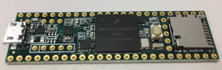
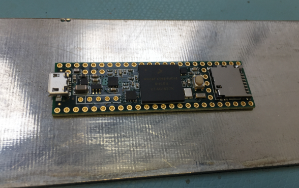
Teensy 3.5 with NXP K64F ARM Cortex-M4F
The only problem? it is not possible to debug it :-(. At least not in the traditional sense. This article is about how to change the board to use it with any normal SWD debugging tool e.g. Eclipse and the Segger J-Link :-).
Outline
The tinyK20 we have produced at the university for student projects are great: small, inexpensive, can be used for many projects and can be both debugged with normal SWD debuggers and can be even used as a SWD debug probe. However with an NXP K20 (ARM Cortex-M4) running at 50 MHz, 128 KByte of FLASH and 16 KByte of RAM it is are not the most powerful board. So somethinig more powerful would be cool!
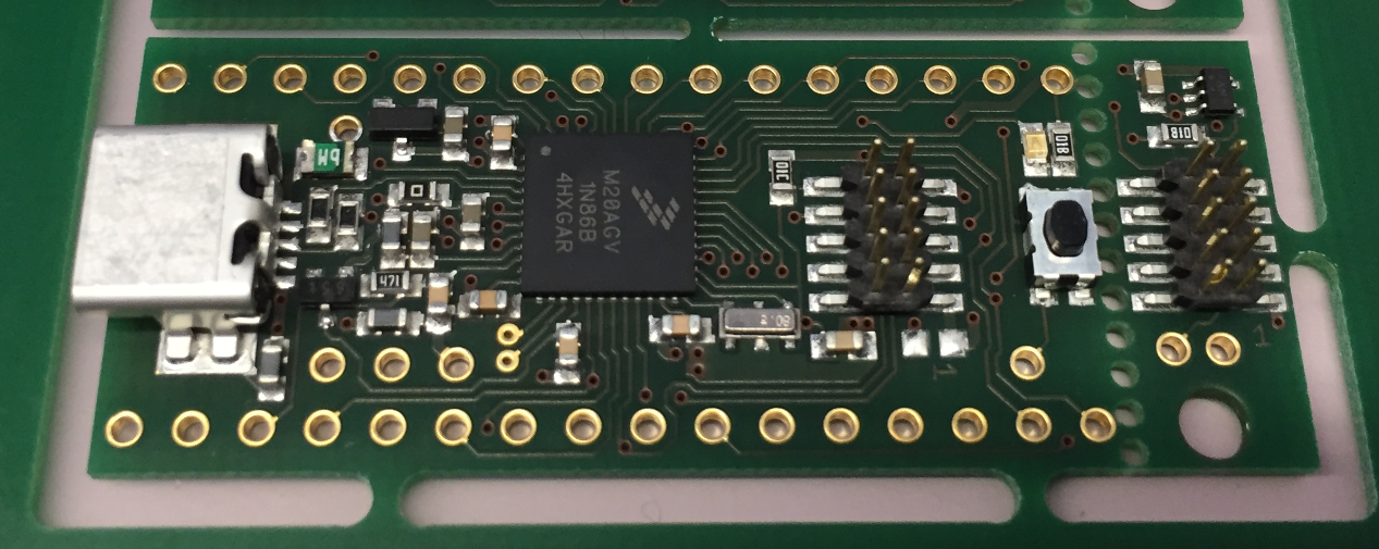
Top Side of tinyK20
The tinyK20 has the option of an micro SD card on the bottom side. Maybe Paul had the same idea, and Hackaday produced an article (http://hackaday.com/2016/08/17/introducing-the-teensy-3-5-and-3-6/) back in August 2016 about two new boards: the Teensy 3.5 and 3.6. The Teensy boards are great (thanks Paul!), but only if using Arduino libraries and the Arduino IDE which never has been an option for me.
Instead, I want to use normal debugging tools like a J-Link. For the Teensy 3.1 I have found a way to do this (see “Hacking the Teensy V3.1 for SWD Debugging“) and we used that for several Teensy boards. But that wiring was not really easy, so we better used the tinyK20 as boards.
SWD Debug Signals on Teensy 3.5/3.6
Now it seemed that Paul finally has added an easier way to to SWD debugging (several asked for that in the forums/community).
From https://forum.pjrc.com/threads/42728-Debugging-strategies:
“For these new Teensy boards, I added a provision to use the debug signals. See the comments and bottom-side photo on the Kickstarter page. There’s a pin you pull low to tell the bootloader chip to tri-state those signals. Drive that pin high or just disconnect (it has a weak pullup) to return to Teensy’s normal mode.”
And from the Kickstarter (https://www.kickstarter.com/projects/paulstoffregen/teensy-35-and-36/comments?cursor=14211857):
“You’ll be happy to hear those test point are on the bottom side. Look for the pads labeled “DD” and “DC”, for Debug Data and Debug Clock. There’s not a lot of room on the bottom side, so had to abbreviate. You might also notice the “DE” pin, for Debug Enable. This pin as a weak pullup. The idea is you pull it low to tell the MKL02 chip to tri-state the debug pins, so you can control them with whatever debug adaptor you use. Just disconnect or drive the pin high to return the Teensy to its normal functionality.”
Well, that sounds great!
Schematics
Below is the schematics of the Teensy 3.5/3.6 from https://www.pjrc.com/teensy/schematic.html:

Schematics of Teensy 3.5 and 3.6 (Source: https://www.pjrc.com/teensy/schematic.html)
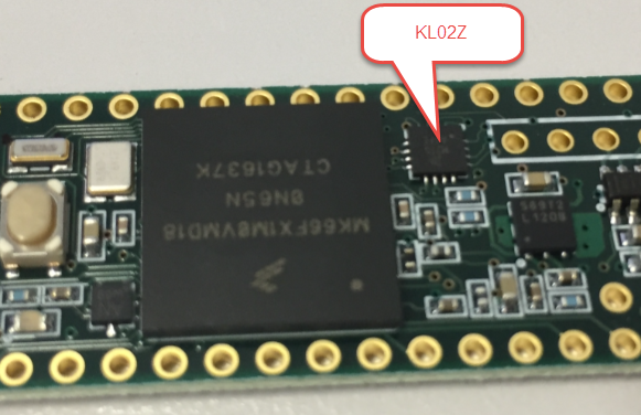
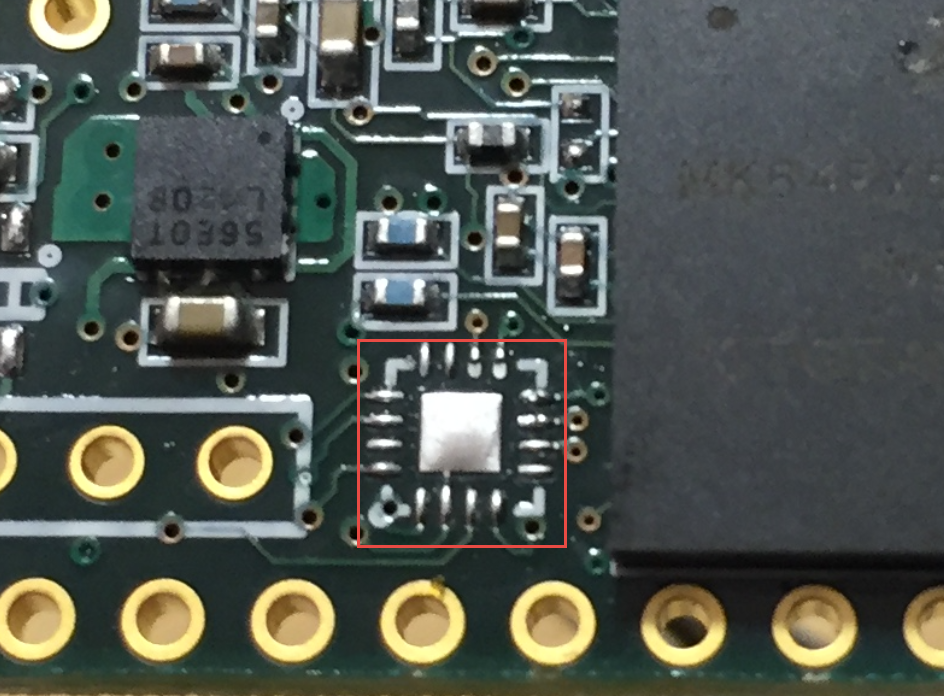
A NXP Kinetis KL02Z acts as the onboard interface and bootloader between the Arduino IDE and the ARM Cortex-M4F on the board. I have marked the relevant signals for debug below (3.3V sense, Reset, GND, DD (Debug Data) and DC (Debug Clock). The DE (Debug Enable) is close to G (GND):

Debug part with MKL02Z32VFG4 on Teensy 3.5 and 3.6
So all what I have to do is to connect DE and G and I should be able to debug it, right?
I need:
- Reset: Optional, but good if the debug probe can force a reset to the device. There is no pull-up on the reset line, as the KL02Z seems to use an internal pull-up
- 3.3V: I need that signal routed to the debug probe, as for example the SEGGER J-Link is sensing the voltage to determine the target device voltate to use the correct voltage levels, plus it can sense if the device is powered. Unfortunately, Paul has not put that signal to the row of ‘debug’ singals (DD, DC, DE, G)
- DD: Debug Data, JTAG_TMS, SWD_DIO
- DC: Debug Clock, JTAG_TCLK, SWD_CLK
- DE: Debug Enable, to be pulled down to tristate the KL02Z debug signals
- G: Ground
Adding Debug Connector
The following picture shows the location of the debug signals on the bottom side of the Teensy 3.5 and 3.6:

Debug Signals on backside of Teensy 3.5 and 3.6
I added a 2×4 SMD Pin header and a 1×5 pin row on the bottom side:
added headers to Teensy
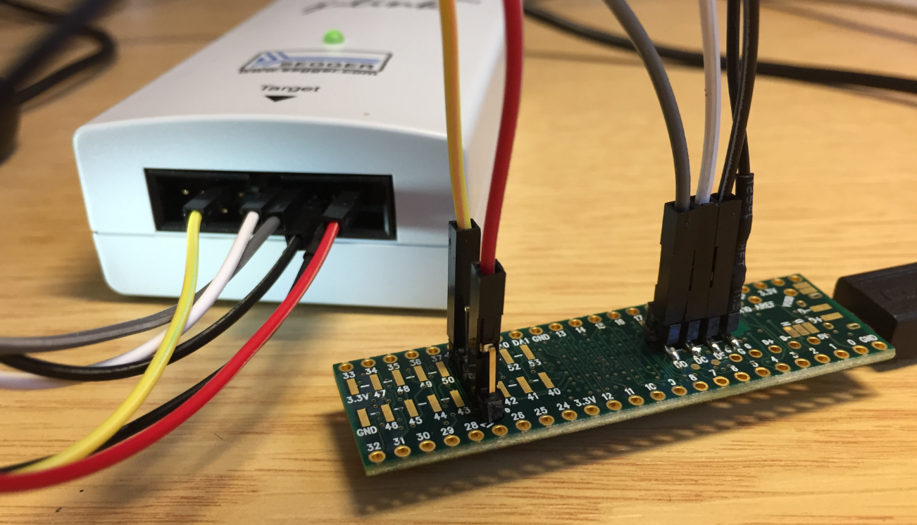
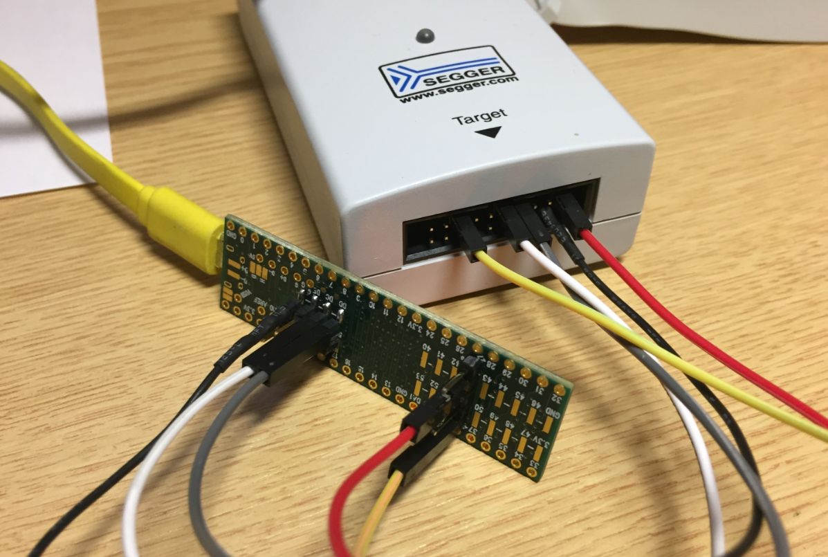
Connection to SEGGER J-Link
I’m using a SEGGER J-Link to connect to the board. The Segger J-Link has the advantage that I can easily connect the signals. The pin out is available on https://www.segger.com/interface-description.html:
JTAG Pins
Below the connected the signals to the Segger J-Link:
First Try to debug the Teensy 3.5
Connection:
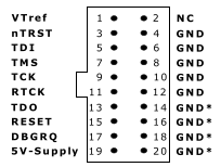
- 3.3V to pin 1 (VTref)
- Reset to pin 15 (RESET)
- G to pin 4 (GND)
- DE to pin 6 (GND)
- DD to pin 7 (TMS)
- DC to pin 9 (TCK)
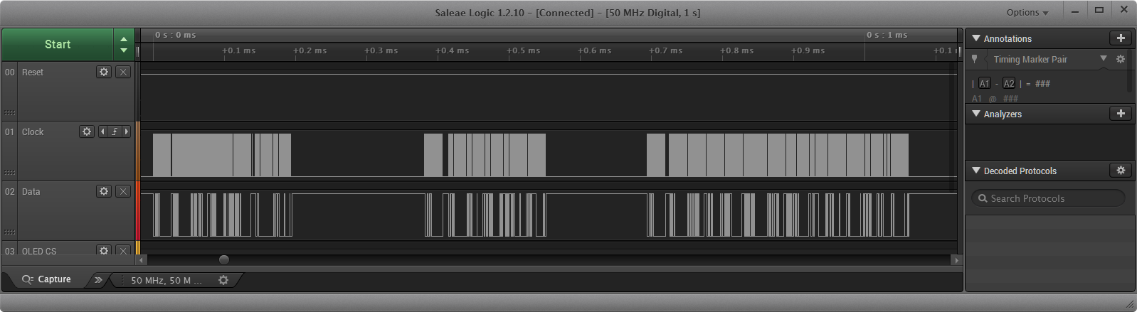
It does not work?
So I tried it out, and I was not able to connect to the board :-(. Looking at the signals it was clear that despite pulling the DE signal low, the Kinetis KL02 keeps sending something to the K64F making it impossible to take over with the J-Link:
Teensy 3.5
It turned out that pulling down the DE signal is still not supported, from https://forum.pjrc.com/threads/42728-Debugging-strategies from 04-24-2017:
“It’s *still* not implemented. Why a year late? Work on Teensy 3.5 & 3.6 (released October 2016) and the USB host library for 3.6 (first release March 2017) pushed that and many other project goals well into 2017. “
:-(.
So what now? Wait again maybe a year or forever? Luckily, I have found a way, but it is the ‘hard’ way.
Modifying the Teensy 3.5/3.6 for SWD Debugging
WARNING: This modifies the Teensy board, and without a doubt you loose any warranty doing that board change!
Pulling the reset line LOW to keep the KL02Z in reset does not work, as the reset line is shared between the KL02Z and the MK66F/MK64F. As anyway the KL02Z on the board is not of any use for me, the decision was to remove it from the board.
Other users report that it is possible to add a 10k Pull-Up on the reset line of the KL02Z. This pulls reset to about 1.85V which seems to be enough to disable the KL02Z.
KL02Z on Teensy
To remove the KL02Z from the board is a bit tricky, below is how Christian Di Battista (thanks!) helped me to get the hardware modification done:
Use something heat resistive and place the board on it:
Board on Heat Resistive Plate
To get the device easier off, use Flux Gel:
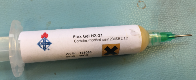
Flux Gel
Apply the flux gel on the pins around the KL02Z:
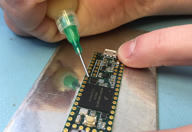
Apply Flux
Video:
Use a hot air station or anything suitable:
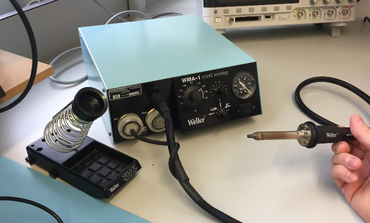
Weller Hot Air Station
Then heat up the KL02Z until it can be removed. Because it has a bottom ground plate, it might take a while until it can be removed.
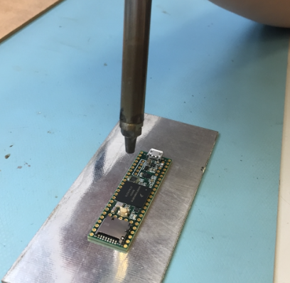
Hot Air
Video of the process:
With the KL02Z removed:
KL02Z removed from Teensy
There is only one thing missing: the reset line needs now a pull-up to 3.3V. One option would be to add a SMD pull-up resistor (e.g. 4.7K) somewhere on that KL02Z footprint. Another simple and easier option os to add a pull-up to the header near the SD card:
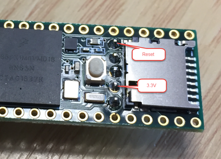
Place for Reset Pull-Up
Finished!
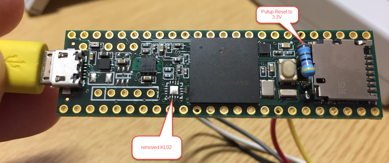
Top Side modified Teensy with pull-up and removed KL02Z
Simplified J-Link Connection
With this, the GND line to DE is not needed any more and can be removed:
Segger J-LInk Wiring to Teensy
💡 If your debug probe does not do any target voltage sensing (as the J-Link does), you don’t need that red Vdd wire. The Reset wire is optional too (but highly recommended), because it is used to reset the target if the processor does not respond on the SWD connection.
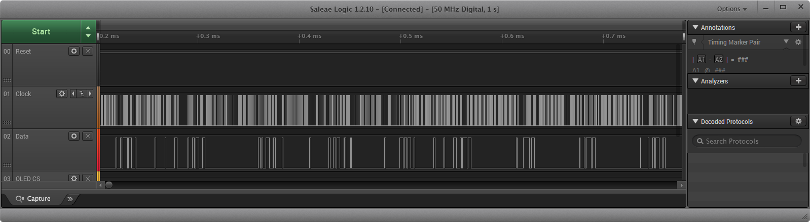
And with this, the J-Link SWD protocol is able to take over the ARM Cortex-M4F :-):
J-Link Communication
Finally, I can debug the Teensy with Eclipse, GDB and standard SWD debug tools:

Debugging Teensy 3.5 with Eclipse and GDB
Another way…
Waldemar Krasovskyy has sent me another variant how to debug the Teensy (thanks!).
He used a ‘quick and dirty’ variant with two pins shorten on the header to connect to the debug pins:

Cut down pins for Teensy debugging
The two pins then connect to the SWDIO and SWDCLK of the KL02Z:

SWDIO and SWDCLK on Teensy
One of his ideas is to use pogo-pins to make the contacts with the SEGGER J-Link:

Pogo Pins
With some headers a connection can be made using the Pogo Pins:
Contacting with Pogo Pins
Another approach is to use and access the signals routed to the SD card:
SD card adapter for JTAG debug on Teensy
Thanks Waldemar for the ideas!
Summary
The Teensy is a great board, and Paul Stoffregen does a really great job. But I really don’t understand why he makes it so hard to use his boards for debugging? Maybe others are used to printf() style debugging as a hobby, but to me this is not the adequate way how to develop for an ARM Cortex-M. To use normal SWD debugging tools with the Teensy 3.5 and 3.6 it requires a hardware change, as for the Teensy 3.1 (see https://mcuoneclipse.com/2014/08/09/hacking-the-teensy-v3-1-for-swd-debugging/). Because the DE (Debug Enable) signal does not work, it requires removal of the KL02Z microprocessor from the board. And because the board does not allow the standard SWD debug header, I have to create a custom cable. It works fine, but is not ideal. I really wish Paul would have provided a normal 2×5 SWD debug header or footprint (ideally on the top side): that would make his boards even more useful.
Happy HotAiring 🙂
Links
- SWD debugging the Teensy v3.1: https://mcuoneclipse.com/2014/08/09/hacking-the-teensy-v3-1-for-swd-debugging/
- Teensy v3.5: https://www.pjrc.com/store/teensy35.html
- Teensy v3.6: https://www.pjrc.com/store/teensy36.html

Hey there, you should submit this to hackaday.com.
They cover stuff like this all the time and would love it.
LikeLike
Hi Kurt,
yes, they do cover such things from time to time. I have posted a response in the PJRC forum to a related questions so Teensy users can find it.
LikeLike
Sounds like an overly complicated way to get debug to work. Why not simply override the pull-down on the reset with a stronger pull-up? Also what you’re doing with the heat-gun is rather risky (lifting up the board with the chip you’re trying to remove), this has a good chance of either killing a trace or knocking off neighbour parts like the resistors… What you typically do here is to isolate the part you want to remove by putting 4 lines of Kapton tape just around the outline of the part. Let the Kapton tape run over the edge of the board thus effectively securing all parts except the one to remove in place. Then heat it up properly and the solder has it’s molten shine carefully nudge the part to see if it moves and only if it does carefully pick it up…
LikeLike
overly complicated: I wish the board would enable debugging, then something like this would not be necessary.
Reset is low active, so I cannot use a stronger pull-down. And a stronger pull-up would not work if I want to get it pulled down by the JTAG debug probe.
Yes, I considered capton tape too, and that would make it even easier, but it worked very well that way for two boards.
LikeLike
I’m quite aware RESET is usually low active which is why there’s usually a pull-up in place. I’ve just checked the schematics and this is certainly not the case. The KL02Z must be actively driving the RESET pin because otherwise it would be floating which is not a good idea und wouldn’t work well. If the software on the KL02Z doesn’t work as intended by not respecting the DE signal that’s quite a pity but I don’t think it would help much anyway because if you disable the active signal from the KL02Z (or set it to open drain) then RESET would be floating without a pull-up somewhere.
However to achieve this very same effect you don’t need to desolder the KL02Z, simply cutting the power supply at pin 1 and adding the pull-up as you did would do just as fine.
LikeLike
Yes, the KL02Z must drive it down, probably it has its internal pull-up enabled too. Cutting the supply to the KL02Z with an added pull-up to the reset line is indeed another option.
LikeLike
Has somebody tried removing the power pin from the KL02Z. Won’t the device then be powered through one of the io pin’s protection pins?
LikeLiked by 1 person
I have not tried that. It worked best for me to remove the KL02Z as it was of no use for me anyway.
LikeLike
Pingback: Adding a debugger to a Teensy 3.5/3.6 | Hackaday
Hy great job.
is it possible to load the arduino code to kinetis studio?
I want to use all arduino libs and to debug the teensy.
LikeLike
I’m using Arduino code, yes. But not directly: I copy the code and make small modifications. It is not possible to use the Arduino code directly as you would need a full port of the wiring library which does not exist to my knowledge. But this is not a big deal, I can use basic pin and utility functions instead.
LikeLike
i see. i use a lot of the teensy library like CAN-Bus and the ADC and Timer Modules.
do you have a small sample project to get some basic knowlage, maybe i am able to convert the visual micro project to kinetis.
LikeLike
Best if you use KDS or the MCUXpresso IDE, start with the wizard to create a new project and then add the source files.
Other than that, I have plenty of example projects on GitHub: https://github.com/ErichStyger/mcuoneclipse/tree/master/Examples
Many of the projects are using originally some Arduino code or libraries e.g. for sensors.
I hope this helps,
Erich
LikeLike
Hi Erich, excellent work! I did replicate your setup. Now I am trying to upload and debug via platformio.org. Any hints on how to configure the IDE? https://stackoverflow.com/questions/45612493/platform-io-upload-to-teensy-3-6-via-swd-j-link
LikeLike
Hi ! Great work, but desoldering a chip on my boards was a no-go, I still want to keep the Teensy bootloader. Instead, I found a much easier way 😀 Just hold the KL02Z in reset…
You said that you tried something like that, but it reset the K66 as well. That’s because you didn’t used the right pin 😉 The reset pin of the KL02Z is pin 15 (PTA1), which is not routed at all. Just solder a thin wire to it and tie it to VSS, and voilà ! 🙂
It should work the same way with the 3.5 and 3.2, and the same principle could be applied for the 3.0/3.1 I think (with the reset pin of the Mini54), although the debug pins are less accessible…
Happy debugging 😉
LikeLike
Thanks for sharing, that’s indeed a very good solution too!
LikeLike
Hi Benjamin,
we tried that approach with pulling downthe KL02Z pin15, but that did not work? Did we miss something?
LikeLike
Hi Erich,
It work for sure, me and some others have tried successfully (there is a thread on the pjrc forum). Check that the KL02Z is indeed reset by trying to upload a code from Arduino, the Teensy Loader should fail. If not, check everything 😉
Might just be a bad solder blob, or wrong wiring.
MattMatic made a nice article on the procedure, with pictures, check it out to verify your wiring (check https://medium.com/@mattmatic/preparing-teensy-3-6-for-swd-b014b0ce2999 and https://forum.pjrc.com/threads/42728-Debugging-strategies?p=159791#post159791)
LikeLike
that will help, thank you!
LikeLike
Hi all,
connecting the reset pin to GND worked for me.
But there is another way to get the KLO2C being non-functional.
Pin 14 and Pin 16 are SWD_CLK and SWD_DIO of the KLO2C. They are routed to test points on the bottom side. These are much easier to solder.
Using an appropriate debug probe (e.g. J-Link) one can erase the contents of the KLO2C. Reading it out before could be a good idea though.
LikeLike
That’s actually indeed a good idea!
LikeLike
Thank you SO much, Erich! I’ve been looking for a lower-priced K66 board and each time I look at the Teensy, I keep balking because I couldn’t hook up a JLink to it.
I understand Paul’s desire to use a bootloader friendly for Arduino users, but I never understood why he couldn’t just include a jumper that allows you to use either the debug port or the Arduino-friendly bootloader.
LikeLike
Hi Robert,
I think Paul’s desire is more about protecting his sales so it cannot easily counterfeit. I understand that desire 100% as he does a great job both on hardware and software. On the same time I think he misses a great opportunity for more sales for his Teensy board. Alone at our university we have produced and used hundreds of tinyK20 (https://mcuoneclipse.com/2015/11/22/data-logger-with-tinyk20-board/) which are basically a Teensy minus that closed teensy bootloader, but have normal SWD/JTAG debug capability. We are usinig the hacked Teensy 3.5/3.6 in several projects, but because that hacking is still painful, we decided to build a new tinyK22 basesd on the Kinetis K22 device with more RAM and FLASH (same device as on the NXP FRDM-K22F).
LikeLike
Hi Erich,
Thanks for these fantastic tutorials!
I followed all the steps you described and unfortunately, I cannot connect my Jlink to the MCU. I checked the reset_b pin with the oscilloscope, and apparently, the MCU is constantly resetting.
I had a look on this link: https://community.nxp.com/docs/DOC-99609 and they say that it is caused by the watchdog which is in continuous enabled mode the first time you turn ON the MCU.
I completed the operation on the Teenzy 3.5 which has never been used before (no Arduino code flashed on it). Should I write some code on the MCU before following the steps of the tutorial?
Thanks in advance and greetings from Lausanne
LikeLike
Hi Raphaël,
it worked for me with Teensy devices which never have been used with the Arduino IDE (I don’t use that IDE anyway with it).
So yes, that reset signal is normal for blank devices, but to me this is not the watchdog, gut the hardfault: the CPU runs, but the reset/vector table is erased with 0xFFFFFFFF, it tries to load this as stack pointer and programm counter, tries to run and then causes a hard fault because the instruction is illegal.
If you have removed the Teensy loader chip, and connected as shown in this article the J-Link signals, you will be able to connect with a J-Link. Maybe you have not correcly connected the signals?
I hope this helps, and greetings from the snow covered central part of Switzerland 🙂
Erich
LikeLike
Thank you for the quick answer!
I already checked the connections and there is no issue on that side. Actually, the LED of the Jlink is orange when all is powered up, but does not seem to be very stable (oscillating like a star…).
Here is the log of the Jlink if it can be helpful:
J-Link RTT Viewer V6.22 : Logging started.
LOG: Global terminal added.
LOG: Device “MK64FX512XXX12” selected.
LOG: InitTarget()
LOG: Protection bytes in flash at addr. 0x400 – 0x40F indicate that readout protection is set.
For debugger connection the device needs to be unsecured.
Note: Unsecuring will trigger a mass erase of the internal flash.
LOG: Executing default behavior previously saved in the registry.
LOG: Device will be unsecured now.
LOG: Found SW-DP with ID 0x2BA01477
LOG: Scanning AP map to find all available APs
LOG: AP[2]: Stopped AP scan as end of AP map has been reached
LOG: AP[0]: AHB-AP (IDR: 0x24770011)
LOG: AP[1]: JTAG-AP (IDR: 0x001C0000)
LOG: Iterating through AP map to find AHB-AP to use
LOG: AP[0]: Skipped. Invalid implementer code read from CPUIDVal[31:24] = 0x00
LOG: AP[1]: Skipped. Not an AHB-AP
ERROR: Could not find core in Coresight setupLOG: RTT Viewer connected.
Thanks again,
Raphaël
LikeLike
Ok, this shows that you are able to to talk to the device with the J-Link :-).
The important message is
LOG: Protection bytes in flash at addr. 0x400 – 0x40F indicate that readout protection is set.
So your device is secured (because erased), see https://mcuoneclipse.com/2012/11/04/how-not-to-secure-my-microcontroller/
So everything is fine. All what you need is now to program your device with a program.
Erich
LikeLike
Thanks again. So it sounds like I have not completely destroyed my Teenzy !
I also tried to program accordingly to your tutorial: https://mcuoneclipse.com/2013/07/22/diy-free-toolchain-for-kinetis-part-3-debugger-gdb-server-with-pe-and-segger/, but unfortunately, I cannot start the Jlink GDB sevrer. I have the following message:
Checking target voltage…
Target voltage: 3.36 V
Listening on TCP/IP port 2331
Connecting to target… ERROR: Could not find core in Coresight setup
ERROR: Could not connect to target
Target connection failed. GDBServer will be closed…
I will also try with Codewarrior,… , to see if I receive a different message.
Raphaël
LikeLike
Don’t waste time with CodeWarrior: it is outdated. Better go with MCUXpresso IDE.
LikeLike
Pingback: First tinyK22 Board with NXP K22FN512 ARM Cortex-M4F | MCU on Eclipse
Pingback: Debugging the Teensy 3.6 with Eclipse MCUXpresso IDE and CMSIS-DAP LPC-Link2 | MCU on Eclipse
Hello Erich,
Do you have any experience with Teensy 3.6 to upload the firmware over the air like with ESP8266? Thanks!
LikeLike
The Teensy board does not any wireless connectivity, so without any transceiver you cannot do any over-the-air update.
LikeLike
Hello Erich, Thanks for the quick reply. Yes, I know that thats why I would use ESP8266 connected to it. Or to make it simple, if we have two teensy connected together, and one has the new firmware(hex file) on its SD card. How is it possible to update the OTHER teensy? And then I can implement myself to ESP8266. Many forum topics says it is possible, but no clear explanation about wiring and code. I have looked the teensy cli, and tried to adopt it on esp8266 but did not work.
  I think not even the wiring is good.
LikeLike
What you need is:
– get the new firmware over-the-air (OTA) to the ESP8266
– have a bootloader implemented on the Teensy
– the bootloader on the Teensy gets the new firmware from the ESP8266
– the bootloader on the Teensy reflashes the firmware on the Teensy
Having said that: that’s a lot of things you have to implement. How a bootloader works: https://mcuoneclipse.com/2013/04/28/serial-bootloader-for-the-freedom-board-with-processor-expert/
I hope this helps,
Erich
LikeLike
Thank you Erich! I will check it!
LikeLike
Here is how I soldered to pad 15 of the KL02Z. The heat to complete the joint was conducted through the single strand of wire I used to make the connection – so it was not necessary to touch the pad itself with a soldering iron.
https://forum.pjrc.com/threads/42728-Debugging-strategies?p=170064#post170064
LikeLike
Hi Robin,
interesting, thanks for sharing!
Erich
LikeLike
it also works completely without soldering. The board has two test pins for KL02 programming. It creates a startup project for KL02 with MCUXpresso and configures reset pin as input with pullup.
LikeLike
That would be good news. Can you share details on this how this is done?
LikeLike
Yes, I can send you a few pictures and the initial project for KL02 by email. If you want, you can also add his inormation to your blog.
Otherwise everything is very simple. The test pads PTA0 and PTA2 by KL02 are in the near of debug connector, and have 2.54mm RM to the USB host connector. I made a 7-pin adapter. 5 pins are plugged to the USB host just for reference to the 2.54 grid. And the remaining two pins are spring contacts. Then you can flash the KL02. PTA4 and / or PTB5 as input with pull up. Done! I also have a jumper between “Prog” and “Reset”, which allows to use the Prog button as a reset button.
LikeLike
Yes, that would be great. My address is erich.styger(_at_)hslu.ch
LikeLike
But we loose the Arduino bootloader by doing that. Somebody willing to create an alternative compatible bootloader ? ^^
LikeLike
There is a standard bootloader provided by NXP in their SDK.
LikeLike
The great attraction of the Teensy, for me at least, is that the boot loader programmed into its seriously teensy KL02Z / MKL02 32 bit microcontroller will enable me to create a product with the Teensy which a non-technical user can update the firmware of, via USB. I haven’t got this far yet, but I have used this facility with someone else’s product (Quicksilver 303) designed with a smaller Teensy. I would create the firmware file in a special format and make it available to my customers. I assume this can be done with an executable produced by GCC, since the QS 303 code was all written in C++ with GCC.
Then the user runs a program on their PC (Windows, Mac or Linux) which is supplied for free by the Teensy team – the Teensy Loader Application: https://www.pjrc.com/teensy/loader.html, of which there are GUI and CLI versions and FOSS source code.
Then the user can update the firmware of the main microcontroller in a minute or two via USB.
I would not like to have to create such a system myself, much less test it extensively on multiple operating systems. As far as I know, this KL02Z / MKL02 firmware is Teensy proprietary. I don’t know of any other such system of firmware and user programs which has this functionality.
The Teensy 3.6, enables me to make products with ready-to-go user-friendly firmware updates and no need to worry about surface mounting the actual BGA ARM 180MHz CPU. It is a minor gotcha that the small microcontroller’s firmware does not allow connecting a standard debugger to the main microcontroller, but that can be fixed with a wire and perhaps some cut tracks. There may be another gotcha in that some of the ARM signals I want are not on the DIP pins, so I would need to solder a few wires into the Teensy PCB, but that is OK
There were plans for new firmware for the smaller microcontroller to enable the main microcontroller to work with an external debug adaptor, but as of 2019-02-15 this enhancement had not been created. Messages 61 and 62 at:
https://forum.pjrc.com/threads/42728-Debugging-strategies/page3
Also of interest:
https://forum.pjrc.com/threads/32922-Purpose-of-MKL02Z32VFG4
View at Medium.com
By the time I get around to developing the product, there will probably be a better Teensy. A 4.0 Teensy is being developed, with a 600MHz i.MX RT1062 MCU. I guess it will have the same USB loading facility. https://forum.pjrc.com/threads/54711-Teensy-4-0-First-Beta-Test/page88
LikeLike
Yes, the bootloader on the KL02 is proprietary, and I think it is that way to prevent cloning the teensy hardware.
Thanks for the link about the Teensy 4.0 which sounds interesting: such a board would be definitely something cool.
LikeLike
In my opinion those custom bootloaders are always a kludge since they either require external hardware or special firmware located at a specific address and precious flash memory. The better approach is to simply use a MCU with a built-in DFU bootloader; those also work with standard utilities (like dfu-util) and won’t cause sweat if they ever break…
LikeLike
It all depends on the quality of the built-in DFU bootloader: they tend to have bugs or do not work well with low power modes or have issues with interrupts. And at the end they are using some internal memory (OTP probably) anyway. Worst case is if the code of such a ROM bootloader is not available. At the end I prefer a good bootloader I can control and have visibility into it.
LikeLike
I’m not sure we’re on the same page here. How can they have problems with low power modes or interrupts? Either they work or they don’t and you won’t have any control over their operation anyway. E.g. the STM32 USB DFU bootloaders work a treat and I couldn’t care less about how they’re implemented or how ST provided the required storage.
LikeLike
If it has working for your flawlessly on STM32: great! My point is that this might not be the same experience for all devices/vendors. For example ROM bootloader code might affect or change the interrupt priorities or have interrupts enabled causing some side effects.
LikeLike
> For example ROM bootloader code might affect or change the interrupt priorities or have interrupts enabled causing some side effects.
I have no idea what you’re talking about. How can disabling interrupts in a completely freestanding firmware have any effect on you? If you’re booted into the bootloader, there’s little you can do except flash code and exit to reset into another boot mode (e.g. execute from RAM or Flash). The bootloader has complete and exclusive control over the MCU and all of its peripherals. Whether it uses polling, interrupts, DMA or random GPIO bitbanging to do its job is completely irrelevant.
LikeLike