
The manufacturing of 200 tinyK20 board is progress, and I’m sharing pictures of it :-).
Rendering from CAD Tool, top side:
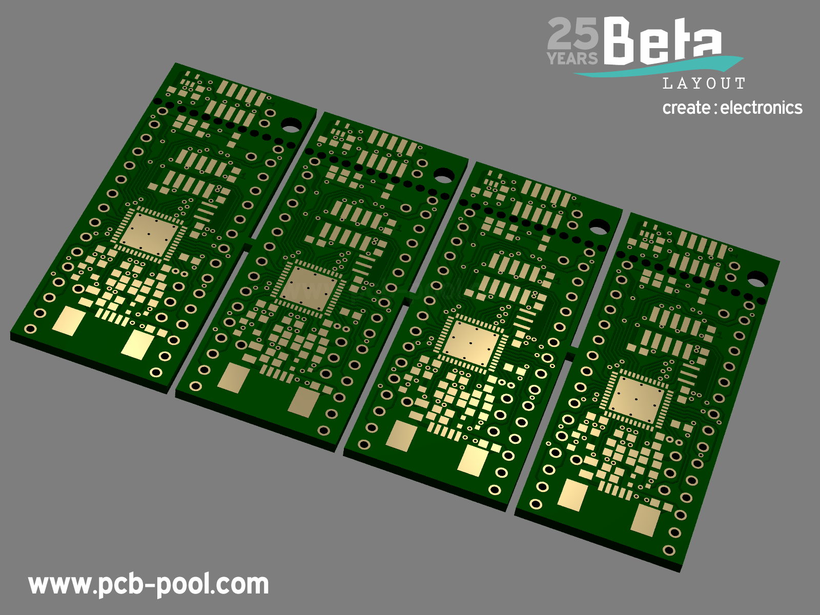
Top side with gold plating and mask
Rendering from CAD Tool, bottom side:

bottom side with gold plating and mask
Bottom side of PCB produced before processing:
tinyK20_PCB_Bottom
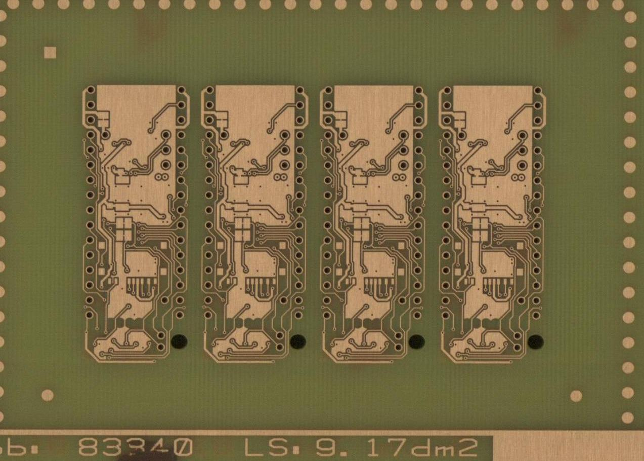
Top side of PCB produced before processing:

tinyK20_PCB_Top
Happy Manufacturing 🙂

Great to hear. Looks a wonderful base to run some dream software on ….
LikeLike
Erich,
Nice layout. Why the string of NPTs?
LikeLike
Hi Bill,
the purpose of the NPTs (Non-Plated-Through-Holes) is to be able to break-off the functionality to debug/connect to another board. For some applications where the board needs to be very tiny and is not used as debug probe, we have that option.
LikeLike
Hi Eric
I have prepared a simulation of the board and also some binary files at http://www.utasker.com/kinetis/tinyK20.html
The boot loader allows software loading via UART1 (SREC format), or using KBOOT (USB-HID) or by drag-and-drop as USB-MSD [all at the same time].
There is a reference application that supports composite USB-MSD to the SD card and USB-CDC, with a menu on UART 1 or the USB-CDC where a USB-CDC to UART 1 bridge can also be commanded (with various other things on the command line interface: memory debugger, low power modes, RTC, etc..)
Regards
Mark
LikeLike
Pingback: tinyK20 Production Boards Ready for Parts | MCU on Eclipse
Pingback: Production tinyK20 Boards arrived! | MCU on Eclipse