
Every day, there is something new to learn. And having problems is always a good learning opportunity :-). Yesterday we were able to find a strange problem with our tinyK20 prototypes, just before we were about to send the design for manufacturing.

Kinetis K20 on tinyK20 Board
Some of the prototype boards did not work properly: the external 32 kHz oscillator was not starting. Resoldering the oscillator or MCU sometimes solved the problem, but not always. Until the problem was found by [Christian Di B.] (thanks!) :-)).
For the tinyK20 board we are using a Kintis K20 (ARM Cortex-M4) in a QFN48 package. The picture shows the device with the bottom ground plane:

QFN48 Kinetis K20
The following picture shows the placement of the package on the board:
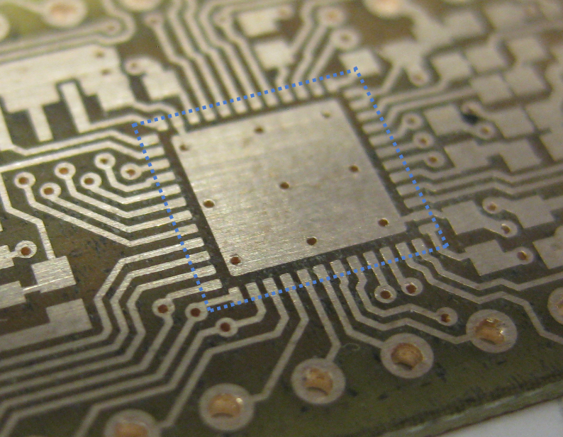
QFN48 Package Position on PCB
Question: can you spot a layout problems in above image? 😉
The QFN48 package looks like this:
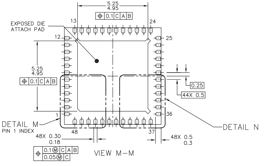
QFN48 Package (Source: Freescale)
What is not obvious right away: On the package of the Freescale Kinetis K20 (MK20DX128VFT5) there is a connection on the outside:

Ground ‘Pad’ on the outside
Yup, looking carefully at the data sheet again, it is here:

Corner Edge Pad (Source: Freescale)
That connection has no real purpose. I believe these pads are from the manufacturing/packaging process. I believe these are just the remainders of something holding the package with the die during manufacturing and then are cut off. The metal contacts are present twice on each side of the package, and are connected to GND (not documented, but easily to verify).
The problem is that in our design we have traces under that ‘edge pad’:

Trace under Edge
It happened that there was some solder on that trace, reaching high enough to connect to the ‘edge pad’ above to make a short cut to GND :-(.

Problem Point
Solder was flowing from the ‘real’ pad to the ‘outside’, and was able to get high enough in some cases to make contact with that ‘edge pad’. And because these ‘edge pads’ were nt easily visible by the naked eye, the problem was not obvious :-(.
Once the problem was identified, it was easy to check/verify the boards :-).
Summary
It is easy to miss tiny and hidden connection points on such small packages. Having traces under the ‘edge pads’ can be a problem, especially with prototype boards without solder mask. The problem is less likely to happen with a solder mask on that trace/pin, but still a potential problem. So we need to change the trace to make sure we do not run into that problem for the boards to be manufactured. And yeah, after the fact things are easy and obvious ;-). I hope that publishing this article might safe someone lots of hours to find the same problem.
Maybe you had a similar problem too? I want to hear about it :-).
Happy Cornering 🙂
PS: thanks again to Christian for his ‘Eagle Eyes’ and for sharing the problem with me.
Links
- Freescale MK20DX128VFT5 Data sheet: http://cache.freescale.com/files/32bit/doc/data_sheet/K20P48M50SF0.pdf
- Freescale QFN48 Package Data Sheet: http://cache.freescale.com/files/shared/doc/package_info/98ARH99048A.pdf
- tiny K20 project: https://mcuoneclipse.com/tinyK20

On some of those QFN packages they recommend no vias on the corners for just that reason, and some QFN packages have more metal on the corners underneath the pad.
Practically in a manufacturing board there would be solder resist that covers the tracks and prevent this problem.
In the technology world moving to smaller and smaller packages and line widths requires process improvements – which unless small size is a requirement of the end product, isn’t always worth the extra technical challenges.
Personally I’ve had problems with K27 QFN debugging, not related to its layout, but it made the whole software testing, circuit verification, assembly and ability to desolder components and resolder less deterministic that I moved to the K27 LQFP package.
For packages pin spacing of 0.65mm or less I always use a solder resist – so thoroughly impressive you managed to get the MK20 QFN running with the no resist .
I’ve been using solderpaste templates from https://oshstencils.com/ – and then assembling components with solder paste and baking in a simple toaster oven following the solder reflow time guidelines and its fantastically easy. However with QFN 0.5mm resoldering/reapplying the solder paste afterwards, through a SolderPaste template is complex. So I’ve considered them one shot boards. A recent plus for using LQFP, I managed to pull off a 144LQP 0.5mm chip with a hot air gun, cuts some tracks that were shorted, and then rebake/resolder it on with enough of the pins working to have made it worthwile.
LikeLike
Thanks for sharing your thoughts and experiences!
Yes, we probably would not have seen that problem with a manufacturing board with solder resist. I have not seen any recommendation from Freescale about traces underneath that area, and maybe missed it. On the other end, maybe this kind of information is not necessary (if we would have been careful enough). We do use solderpaste templates too, but not for this kind of prototypes and small series.
LikeLike
A 5X – 10X microscope with plenty of bright light is very helpful. Every lab should have one.
LikeLike
Yes, something like this is absolutely required. We do have a good microscope to find such problems too.
LikeLike
I designed my first MCU board during waiting for MCU delivery (many years ago). PCB was delivery on the same time as MCU and with big surprise I discover that they do not fits and there exist at least three sizes of TQFP64 package (differs by pin spacing and package size). So, I have to design new PCB. With assembled new PCB I discover that I forget on programming connector. Soldering wires on MCU legs with 0.5mm pin spacing under microscope is big fun. Believe me or rather not. 😉
LikeLike
A classical one 😉 That reminds me about the time when I have built/populated about 10 boards, with each of the QFN packages put in place rotated by 90°, because the ‘pin 1’ marking was not not clear. Outsch!
LikeLike
I suspect nearly 60% of self teaching in electronics is through “almost” simple mistakes like yours.
(Another 30% is spending countless hours reading and trying to figure out what a manual or tutorial is trying to say. The last 10% is putting the project together so it works.)
The only solution I have found to getting something out the door is passion, determination, and constant “creative problem solving” as described in this article and your comment.
LikeLike
Yikes! That would be a hard problem to find. Thanks for letting us know about it.
LikeLike
Hi Erich,
Check out http://www.myropcb.com for both prototype- and production-volume PCBs. I have not found better value anywhere.
LikeLike
Thanks for suggesting that site. $20 for 5 PCBs is a great deal. It is also good to know they are “UL certificated”. 😉
LikeLike
Thanks for that link! We have mostly used http://www.pcbpool.com, but myropcb looks interesting too.
LikeLike
Would a dab of Teflon tape over the corner have worked as a quick fix or troubleshooting technique?
LikeLike
Why don’t your prototype boards have solder mask? I’ve not found the cheap prototyping places charging extra for soldermask.
LikeLike
We manufacture them internally with a laser cutter which etches the copper away.
LikeLike
Ah, that makes sense. That’s a rather slow and expensive way to make PC boards, but it probably reduces your turnaround time by a few days. There is a faculty member here who likes to use a computer-controlled router for making prototype PC boards, but he’s not usually doing fine-pitch surface mount devices.
LikeLike
Not sure if a turnaround time of a few hours I would consider as ‘slow’?
LikeLike
Turnaround is good, but throughput is poor with routers and laser cutters.
LikeLike
Agreed, and that’s why we use it for the first prototype(s).
LikeLike
I’m not familiar with making a board using a laser cutter. I’m familiar with the router (milling) approach. Please tell more about the laser: process, machine, technology, etc. Is this selective exposure of photo resist using an X-Y light source? A separate post would be fine.
Thanks!!
LikeLike
Hi Dave,
see this: https://www.youtube.com/watch?v=mzmjGz0_joM
Erich
LikeLike
Thanks a lot.
LikeLike
Pingback: Fail of the Week: Marginally Documented Pad Shorts to Maskless PCB | Hackaday
I’m not sure it was worth revising the design, being that a solder mask would prevent it, and production boards would have a solder mask. Production boards will have a solder mask, right?
Still, an interesting read, and a great tip for those who prototype on bare boards. Kudos!
LikeLike
Hi Pete,
yes, we had this discussion as well. And while it would have been good to change the design (just to follow the rules), we don’t have to change it, as we will use solder masks for the production batch anyway. But as we (and the students) do a lot of one-off and prototyping witout solder mask, I thought it was worthwile to publish the possible problem so it can be avoided.
Thanks!
LikeLike
I’ve been there and done that too. I had a signal that was being shorted to ground. I happened to place a via for that signal right below this less-than-obvious ground connection on the side of a QFN-16 part.
I found the location of the short with a voltmeter. The signal was a digital output of a Kinetis, and I measured a few mV when it was logic high right at the pin of the micro. As I measured along the trace, it was essentially 0V from that via on. I thought at first it was a PCB fabrication issue until I flipped the board and found the short to the QFN package.
As an aside, I’m thankful for the fault tolerant GPIO ports of the Kinetis. After fixing the short, that pin on the Kinetis was fine.
LikeLike
Yes, when I looked at the package with that ‘really-not-that-obvious’ ground plate extension, I was thinking that this could have been a problem too. Too many traps and holes 😦
LikeLike
Pingback: Board Bring-Up Tips, GDB Logs and Traces in Eclipse | MCU on Eclipse
How is that PCB made ?
LikeLike
With a PCB laser etching machine.
LikeLike
I mean , I see plated holes, are those done in-house? If yes how ?
LikeLike
The through-hole plating is done by an external company doing it with the usual electro-chemical way.
LikeLike
Pingback: Fail Of The Week: When the Epoxy-Coated Chip Is Conductive | Hackaday