
The STMicroelectronics STM32F103 (ARM Cortex-M3) Nucleo boards include the on-board ST-Link v2 circuit which allows to debug the board. This circuit is similar to the OpenSDA circuit found on Freescale boards. Unlike the Freescale OpenSDA, the ST-Link is only the ST-Link: it is not possible to load a P&E Multilink or Segger J-Link or firmware on it. Luckily, the ST-Link has a SWD connector, but this connector is a non-standard one. So how can I debug that board with an Eclipse based environment with GNU ARM Eclipse plugins and a Segger J-Link?
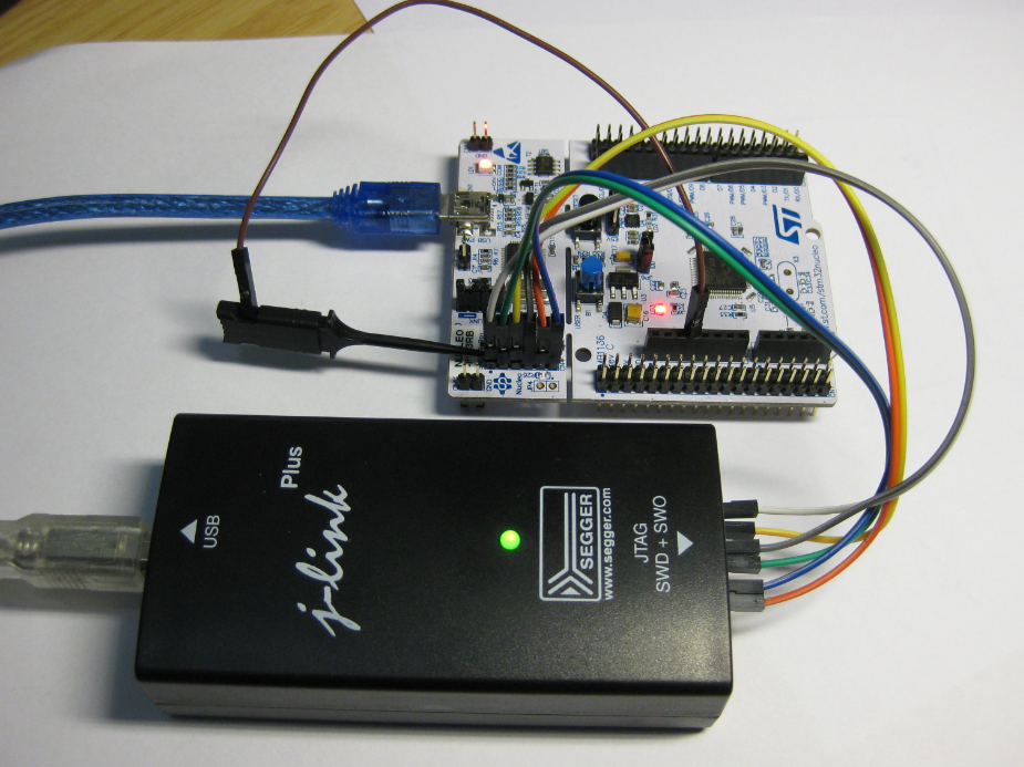
Connected J-Link with Nucleo Board
Overview
In this article I show how to debug the STM32F103RB Nucleo board, using an Eclipse Mars based distribution with and a Segger J-Link. Using the Segger J-Link with a Nucleo board, it requires to connect to the SWD connector on the ST-Link side of the board. The steps described here can be used for any other Nucleo board, as they should have the same SWD connector.
Hardware Connectionc:\tmp
The ST-Link v2 part of the Nucleo board has a 6-pin (CN4) header which can be used to debug the STM32F103RB on the Nucleo board.
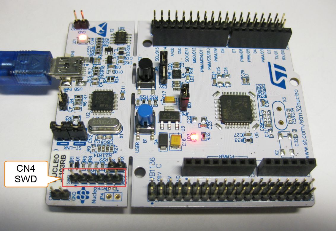
STM32F103 NUCLEO Board with CN4 SWD Header
The CN4 connector has the following pins:

Nucleo CN4 SWD Connector (Source: STMicroelectronics NUCLEO UM1724 User Manual)
The Segger J-Link uses the ‘standard’ 20 pin adapter (see https://www.segger.com/interface-description.html):
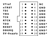
Segger J-Link Pinout (Source: Segger)
I’m connecting the Segger J-Link to the STM32 board like this (colors refer to the cables shown in the pictures):
| Segger | Nucleo | |||
| 1 | VTref | White | 1 | VDD_Target |
| 4 | GND | Yellow | 3 | GND |
| 7 | TMS | Grey | 4 | SWDIO |
| 9 | TCK | Green | 2 | SWCKL |
| 13 | TDO | Blue | 6 | SWO |
| 15 | Reset | Orange | 5 | NRST |
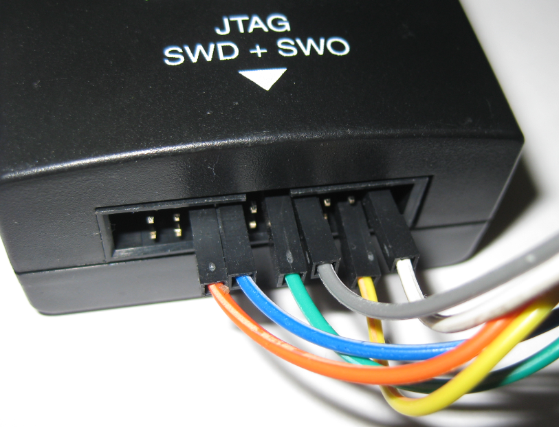
J-Link Connector
Pin 1 is on the top on the right side. The lower row of pins are connected to GND (except the first one, pin 2). The yellow cable shown in the picture is toe connect GND to the Nucleo board, so any of the lower row pins (except the first one, pin 2) can be used.
Connected J-Link with Nucleo Board

SWD Connector on the Nucleo Board connected to J-Link
So far so good: I need to tell to the Segger J-Link that the CPU is powered (VDD_Target): The J-Link senses the power of the target with VTref (Voltage Target Reference) pin. On the Nucleo board that pin on the CN4 header is not powered: the Resistor R9 (near the connector) is not populated on the board.

CN4 SWD Connector Schematic
I think the idea would be that the ST-Link would control it with the AIN_1 signal, but again, it is not connected. The easiest way is to provide 3.3V from the Arduino Header 3.3V pin (brown cable in the picture):
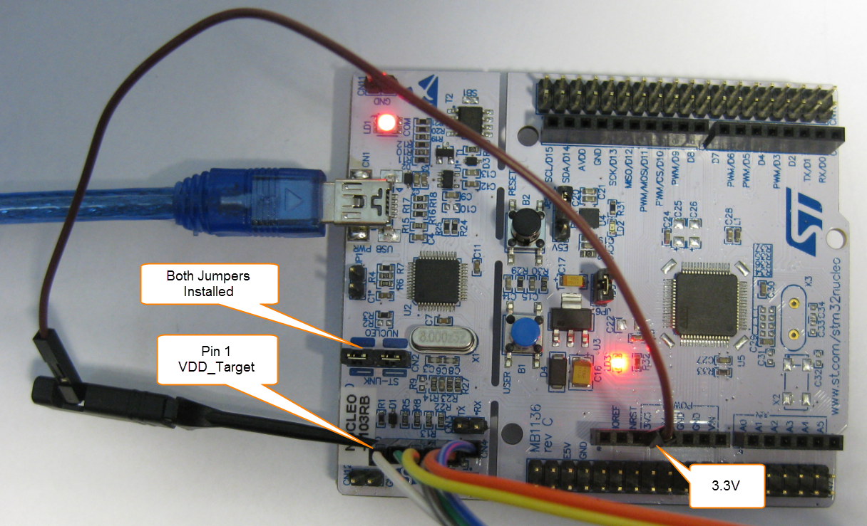
Routing 3.3V to VDD_Target
Project Creation
The GNU ARM Eclipse Plugins come with project wizard and templates for the STMicroelectronics devices.
To create a new project for the STM32F103, I use the menu File > New > Project:

File New Project
I could have selected ‘C++ Project’ or ‘C Project’ too. I I have selected ‘Project…’ then I can now select the kind of project:

C Project
I give a project name, select the device with the toolchain:

New STM32F103 Project
If using semihosting (do not forget to have it turned on in the debug configuration), Trace output can be enabled. If not using semihosting, it can be set to None:

Target Processor Settings
The next dialogs I can keep with the defaults, so click next finish and create the project.
Build the project, and there should be no errors.

Project Created
Debugging
Open the debug configurations and create a new configuration for Segger J-Link. I use
STM32F103RB
as the device:
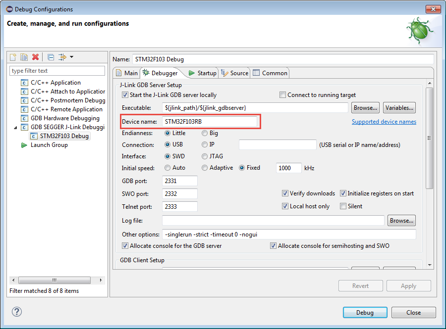
Debug Configuration for STM32F103RB
With this, ready to debug. And voilà I’m able to debug the Nucleo board with the Segger J-Link:

Debugging Nucleo Board with Segger J-Link
Summary
The STMicroelectronics board has an onboard ST-Link debug interface. To debug it with another debug probe like the Segger J-Link, I have to connect the debug probe with the SWD connector on the ST-Link side. Because that connector is non-standard, I need to create a special cable/connector for it. This allows me to use a standard SWD probe with the Nucleo board.
Links
- STM32 Nucleo 64 Reference Manual: http://www.st.com/web/en/resource/technical/document/user_manual/DM00105823.pdf
- STM32F103RB Schematics: http://www.st.com/st-web-ui/static/active/en/resource/technical/layouts_and_diagrams/schematic_pack/nucleo_64pins_sch.zip
- Segger J-Link Debug Probes: https://segger.com/jlink-debug-probes.html

> As the debug connector does not include trace, I have the Trace output option disable:
Why do you think so? With any compliant JTAG/SWD connector the semihosting (debug and stdout) trace channels are always available. Even more, since you connected the SWO too, the ITM trace channel should also be available.
In GNU ARM Eclipse parlance ‘trace’ is not the multi-wire ARM special connector, but just a small family of debug functions (like trace_printf()), completely separated from POSIX syscalls or anything else, that can be used for debugging purposes.
LikeLike
Hi Liviu,
maybe I’m wrong, and probably I made a wrong conclusion. But I had the problem that if I had trace enabled, the program was got stuck in call_host(), called from _trace_write_semihosting_debug(), called from trace_write(), called from trace_puts(). So what did I wrong?
LikeLike
are you sure you enabled semihosting for the J-Link GDB server?
LikeLike
Yes, I’m pretty sure I had it enabled. I will check again tomorrow morning and report back.
LikeLike
Hi Liviu,
my bad! And embarrassing 😦 I was sure I had semihosting turned on in the launch/debug configuration. Checking again this morning I see that semihosting in the debugger setting was disabled. Turning it on, and things are working as they should 🙂
I have to update the post to relect this.
Multumesc mult!
LikeLike
😦
I noticed in older posts you were over-conservative regarding semi-hosting and suggested to turn it off (https://mcuoneclipse.com/2014/02/16/diy-free-toolchain-for-kinetis-part-10-project-creation-with-gnu-arm-eclipse-2-1-2/), but I don’t concur to this, when used properly, tracing, via ether semihosting or SWO, is a powerful debugging mechanism.
LikeLiked by 1 person
Nice post! Have a blog post idea.. Compare the speed and feature set of each debugger type. To see if there is a measurable benefit in buying a dedicated debugger vs opensda/St link/lcp link etc
LikeLike
Thanks! 🙂
I have some numbers here (OpenSDA vs. J-Link):
The numbers might be somewhat better today, but the difference between a J-Link and OpenOCD is by factors.
Again, there is now OpenOCD 0.9.0 which is supposed to be better. I’m a big fan of open source, but it has to work. OpenOCD simply did not do that for me: it was slow, and it was unreliable. I rather buy for 60 Euro a J-Link EDU and this saves me a lot of frustration. Regardless, I keep an eye on OpenOCD, and I have especially an eye on pyOCD which seems to work better. The good thing with ARM devices is that commercial run control solutions are affordable, there are ‘free’ solutions from the vendors (ST-Link, OpenSDA) and there are open source solutions (CMSIS-DAP/OpenOCD/pyOCD/USBDM) 🙂
LikeLike
Great post, thanks:-)
LikeLike
HI Erich,
Is it possible to use TinyK20 to debug STM32F103RB ?
LikeLike
Hi Zohan,
I have not tried it, but with the ARM CMSIS-DAP application I think it would be possible.
Erich
LikeLike
I was trying to use K20 to program STM32F4 on COOCOX but it can’t work properly. 😦
LikeLike
Well, the K20 is very innocent: what you need is to run the proper CMSIS-DAP with the correct device support (flash programming/etc) for your device.
LikeLike
Hi, Erich! Recently I started working/studying with a STM32 board, the STM32F407 Discovery board. I’ve found some good works using it on the internet, but I would like to know if you have knowledge of another blog, youtube channel or any other kind of material with focus on that platform as you do here with Kinetis. Anyway, thanks for everything. Your work here helped me a lot this last year!
LikeLike
Hello Erich,
Do you have any experience with Segger J-Link OB (on-board) probes? Are they really the same as regular J-Link devices?
I want to use ST Nucleo board with Segger’s ST-LINK On-Board firmware but I am not sure if that is the best approach. Segger website says that ST-LINK On-Board is fully compatible and has the same features as J-Link OB. On the other page they say that J-Link OB is an on-board debug probe that is again fully compatible and has the same features as regular J-Link.
https://www.segger.com/products/debug-probes/j-link/models/other-j-links/st-link-on-board/
https://www.segger.com/products/debug-probes/j-link/models/j-link-ob/
As I understand this implies that ST-LINK On-Board is the same as regular J-Link, but it might be a stretch?
LikeLike
According to that description on https://www.segger.com/products/debug-probes/j-link/models/other-j-links/st-link-on-board/, this is what vendors like NXP, Freescale and STM (and others) have put on their evaluation boards. I’m using this interface a lot and I’m very happy with it. It acts like a normal J-Link debug device. The difference from an external probe is (from what I can tell) that it only can be used with that evaluation board (a license dialog asks to confirm this), it does not have extra voltage sensing (e.g. to work with other than say 3.3V targets) plus in my experience it is not as performant as the normal J-Link debug probe, simply because usually a less powerful on-board device is used (e.g. the K20 for OpenSDA or the one for the STLink). With normal debug operations you probably won’t notice much of a difference, but I saw a difference e.g. using the Segger RTT or Segger SystemView (or Percepio Tracealizer): tracing and sending lots of data is much better if you have a ‘real’ J-Link probe. Other than that, I’m very happy with it.
LikeLike
Erich, thank you very much for your prompt and comprehensive answer, I really appreciate it, and I have another question for you.
How would you compare J-Link OB to CMSIS-DAP firmware variants? I know that former is Segger’s proprietary and the later is ARM’s open solution, but is there any real difference (performance, reliability, features) for basic debug operations?
Few evaluation boards with on-board debug units have options to replace original debug firmware with either J-Link OB or CMSIS-DAP so I am wondering how those two compere for normal debugging. I know there is a big difference in additional and proprietary feature support, but is there any noticeable difference or advantage in regular use?
LikeLike
First off: this is my own and personal opinion, based on my experience. In most cases, the J-Link firmware is much better, faster and reliable than the CMSIS-DAP firmware. Additionally, it features many more tools with the installed Segger applications, from RTT to flash programming and command line tools. The CMSIS-DAP (using the LinkServer) has some advantages if used with the NXP MCUXpresso IDE), but otherwise the J-Link one is really superior. Plus it supports ‘unlimited breakpoints’ which is a great value add. And this greatly simplifies debugging.
Additionally, to me the Segger firmware is much faster to debug with than with the normal CMSIS-DAP variants.
There is just one caveat: the Segger OB firmware usually cannot be used for your own boards: it is licensed only with the vendor evaluation boards.
LikeLike
Erich, thank you for a great answer!
LikeLike
Hello,
for some time it has been possible to convert the on-board ST-LINK to J-Link.
https://www.segger.com/products/debug-probes/j-link/models/other-j-links/st-link-on-board/
LikeLike
Yes, I have done that too. Do you believe this is not possible any more?
LikeLike
What are the advantages of using an external j-link instead of the built-in stlink swd?
Also, don’t the CN2 jumpers installed connect the built-in st-link f103 to the main cpu? How is it that there’s no conflict between the external stlink and the built-in?
Thanks!
Ben
LikeLike
Hi Ben,
Using a J-Link in general has many advantages over using an STLink: it is faster, has more features, can be used with tons of other tools, comes with RTT and SystemView, …
The onboard STLink can be reprogrammed as a J-Link too (this is what I do most of the time anyway), see https://www.segger.com/products/debug-probes/j-link/models/other-j-links/st-link-on-board/
Using an external probe is usually faster too (more powerful processor than the onboard debug device), plus it gives me SWO (see https://mcuoneclipse.com/2016/10/17/tutorial-using-single-wire-output-swo-with-arm-cortex-m-and-eclipse/)
About a possible conflict: this all depends on what the onboard debug device does: by default if it is kept in reset, the output lines are tristate so there won’t be any conflict even if electrically connected. If in doubt or of that does not work, it is of course better to disable/cut the lines.
Erich
LikeLike
Hi Erich,
What is the name of the component you used to attach the 3.3V from the Nucleo board to SWD pin 1? (the black ‘probe-looking’ device). I would like to know where to buy one.
Thanks
LikeLiked by 1 person
Hi Ryan,
that one was one of the clamp connectors I have received with my Salea logic analyzer. You can find such connectors if you search for ‘logic clamp connector’ or ‘test hook clips’.
LikeLike