I *love* the Freescale Freedom boards, and you probably recognized that with all my projects using them. The Freedom boards are small, inexpensive and can be easily extended with Arduino shields which makes them a great platform for prototyping. But sometimes I just need an ARM microcontroller with some headers, and then the 85mm x 55mm size of the Freedom board is not ideal. That’s nothing new, but I realized that yet again when I did my Adafruit NeoPixel clock: the FRDM board was rather bulky, even if hidden behind that clock. I need something much smaller: the Teensy board!
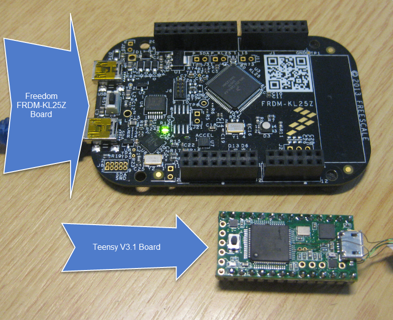
Size Comparison FRDM vs. Teensy
Meet the Teensy V3.1 Board
I have met the Teensy board the first time when it was featured on Hack-a-Day with the 3.0 and later with the 3.1 version. The Teensy V3.1 board (https://www.pjrc.com/teensy/index.html) is a tiny 35×17 mm board (Hint: the board name tells it all!) with following main features:
- Freescale K20DX256 ARM Cortex-M4 Processor (72 MHz, 256 KByte FLASH, 64 KByte SRAM)
- MINI54TAN Bootloader Device, an ARM Cortex-M0 (see this thread) which acts as USB Bootloader
- Prog Button, connected to the Nuvoton MINI54TAN
- A User LED, connected to the K20
- USB port connected to the K20. The board supports by default USB device class, but can be modified for USB host functionality (I have not tried that yet).
- Pins on outer headers and lower pin pads, bread board friendly
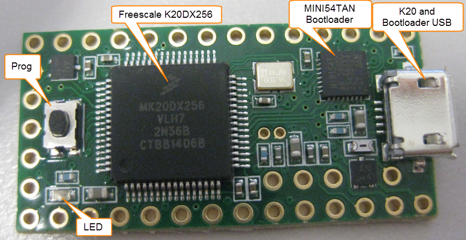
Teensy v3.1 Top Side
On the backside the board is prepared for a 32 kHz oscillator and USB host mode. Additionally it features added pin pads and various test points:
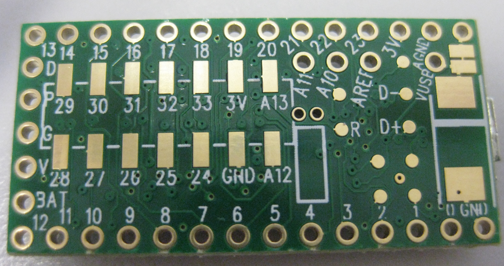
Teensy v3.1 Back Side
The schematics are found on https://www.pjrc.com/teensy/schematic.html. The board costs below US$20 and can be ordered from multiple sources (I ordered mine from Adafruit (https://www.adafruit.com/products/1625)).
No Debug?
So far so good. I was very reluctant to order the board because it has a problem: It does *not* expose the JTAG/SWD debug pins :-(. That means, it is not possible to debug the ARM processor on that board with the usual JTAG/SWD debugging tools.
💡 Maybe it is just me: I respect the ‘Arduino way of programming’, but it is just not the way I think development should be done. I need full control of the hardware which includes deep inspection (debugging) of the application. Because in my experience the hard problems (and there are many!) of embedded development can only be solved with good debugging tools.
Instead, a USB based bootloader is used, the Teensy Loader (https://www.pjrc.com/teensy/loader.html). With that loader programs can be loaded to the board, but it does not allow me to debug the board by any normal means. That topic is discussed in the forums too (see http://forum.pjrc.com/threads/6-JTag-on-Teensy). So the board is open, but not that bootloader on the MINI54TAN device. Not having the JTAG/SWD pins exposed at least on test pads on that great board is definitely a pity.
💡 I only can speculate that Paul Stoffregen (https://www.pjrc.com/about/about_us.html) want to protect the board IP from beeing cloned, which I can understand. But why not at least expose testing pads for JTAG/SWD?
Adding SWD Debugging
❗ WARNING: of course, any change of the Teensy board like this will void any warranty!
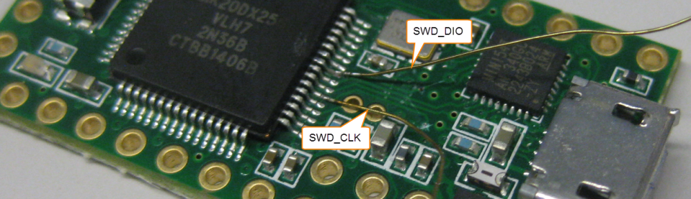
Looking at the schematics and the board layout under the microscope, it was clear that it would be possible to add SWD debug functionality to it. As SWD only needs 5 pins (GND, 3.3V (power sense), DIO, CLK and Reset, it should not be too hard to route it to a standard 10 pin SWD/JTAG header:

SWD Header Pinout (Source: FRDM-Kl25Z Schematics)
So I checked the schematics (https://www.pjrc.com/teensy/schematic.html), and all the signals are available, and SWD_CLK is on PTA0, and SWD_DIO is on PTA3:
💡 To keep things simple, I only used the SWD pins, and not the two additional ones for JTAG (PTA1_JTAG-TDI and PTA2_JTAG-TDO), but that would be certainly doable with two extra wires.
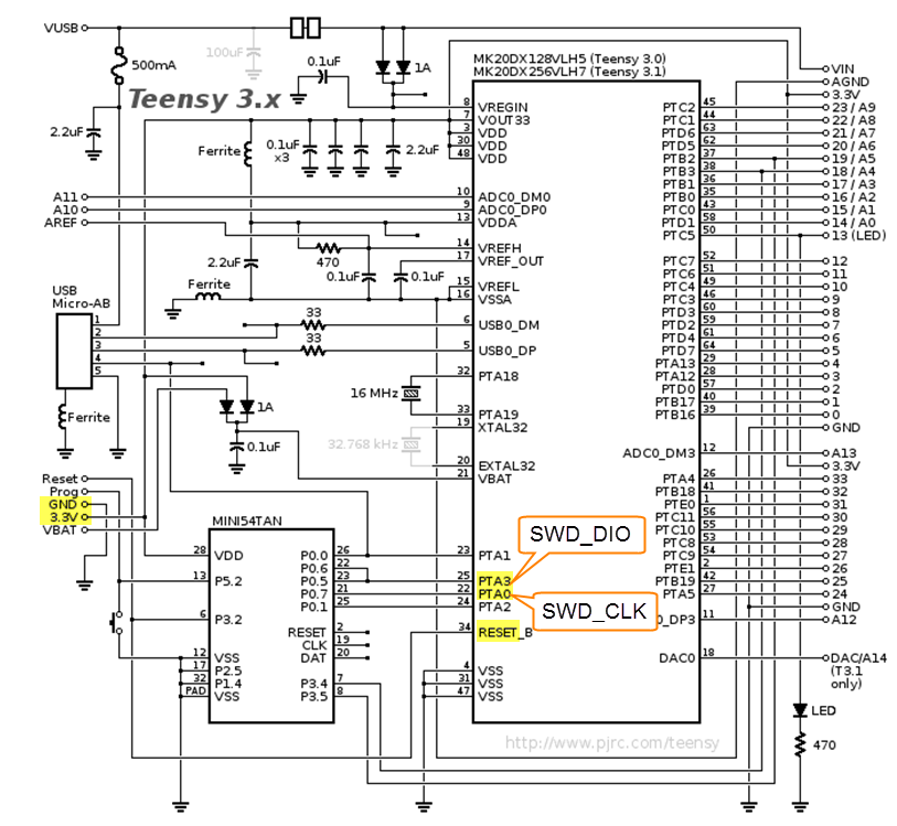
Teensy v3.1 Schematic with SWD Pins (Source: based on https://www.pjrc.com/teensy/schematic.html)
💡 Interestingly, the USB DP and DM pins are *not* connected to the MINI54TAN device, but it manages the bootloading to the K20 through USB? I belive upon press of the ‘Prog’ button, the MINI54TAN programs a small USB bootloader program to the K20 which then runs the update? Would be an interesting approach just to use a single USB connector.
- 3.3V andGND are easily available on the back side oftheTeensy:
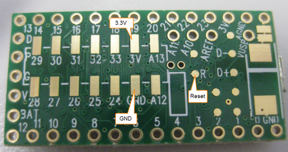
3.3V, GND and Reset on Teensy 3.1
- For SWD_CLK and SWD_DIO there are no easy accessible pads. But an inspection of the layout of the board suggested to cut the traces to the MINI54TAN and solder wires directly to the K20 pads.

💡 The idea to remove the MINI54TAN and to use its pads has been considered. But then this would be a non-revertible change (or at least not easy). So cut two traces and wire some wires sounds the better approach. Maybe cutting is not necessary, but I did to isolate it just in case.
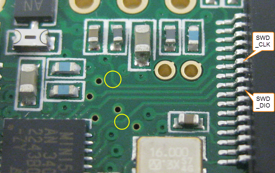
SWD DIO and CLK Traces on Teensy V3.1
💡 NOTE: as discussed in the comments section of this post, there is an *easier* way to get SWD debugging for the Teensy 3.1, without the need to cut wires: The idea is to pull down the Reset line of the TAN chip. The reset line is located nearby the pin 1 on the backside of the board. Install a jumper to put that line to GND to enable SWD debugging :-).
TAN Reset Pad

With this, wires get soldered on the microcontroller K20 pads (use soldering flux and head the pin with a wire wrap wire):

SWD_CLK and SWD_DIO Wires Soldered to the K20 Pins
Then cut the traces to the MINI54TAN:

Cut Traces to MINI54TAN
💡 Tried to use SWD without cutting the two lines, but this does not work. So indeed, the lines has to be cut, as the MiniTAN is affecting the SWD communication.
Compared to the previous step, the 3.3V, GND and Reset wires on the backside of the board are easy:

Soldered Wires on Back of Teensy 3.1
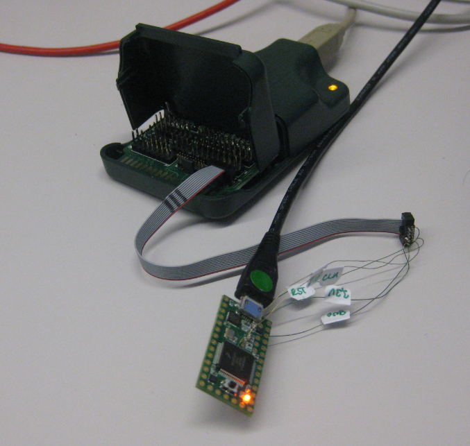
Next step is to connect the wires to the normal 2×5 pin SWD/JTAG pin header (or an adapter to it). I had a header with cable at hand, I decided to solder the wires to header.
💡 The pin pitch is rather small. Next time I better create a small adapter PCB which would make soldering easier.
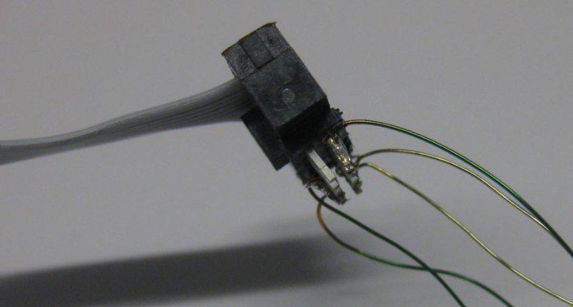
Soldered wires to 2×5 pin SWD JTAG Header

Pins on SWD JTAG Header
With this, I was able to debug the Teensy V3.1 with a normal JTAG/SWD hardware debugging tool, and within minutes I had a Processor Expert blinking LED program made with Eclipse plus GNU ARM tool chain running on the Teensy:
Debugging the Blinky on Teensy 3.1 with a P&E Multilink
Now with this that board is finally useful for me: I can debug with my favorite Eclipse tools :-).
Summary
The Teensy V3.1 is a fabulous board, with a processor I love: an ARM Cortex-M4 powerful for most of my projects. The board is tiny and small. The bad thing is that the usual JTAG/SWD pins are not available either on the outside or on test pads, making JTAG/SWD debugging not possible by default. But with some hacking and good soldering skills, a Teensy board can be turned into a board which talks with a JTAG/SWD cable like a P&E Multilink or Segger J-Link. And then the board can be utilized with an IDE like CodeWarrior, Kinetis Design Studio or a DIY Eclipse ARM Toolchain :-).
💡 My wish is that future Teensy boards have at least the footprint of a standard 2×5 JTAG/SWD header on it, with some isolation traces. That way I can solder a header, cut a few traces and I have a board I can debug with the tools I’m used to. And if I have an extra wish: Replace the MINI54TAN with a Kinetis K20 running OpenSDAv2.1 as on the Freedom boards, and the Teensy would be the perfect board for me: a small and tiny open source board with an open source bootloader and firmware 🙂
Time to use that board now for my projects….
Happy Teensing 🙂

Hi, Erich.
Great site.
If I replace the Teensy 3.1 MINI54TAN with a Kinetis K20 from the Freedom board running OpenSDAv2.1 , would it work at this time?
We need to ask prjc to do an upgrade to teensy 3.1 with SWD.
Thanks, Manuel.
LikeLike
Hi Manuel,
yes, that would work (but the footprint of the MINI54TAN would not be the same, so you cannot swap this out without a board change).
I already have asked prjc for SWD support, and I know others had asked the same if I browse the forum). I’m wondering: why not just make a Teensy compatible board, but with a K20 and OpenSDAv2 on it? My estimate would be that such a board in 100-500 quantities should be doable in the $10-15 range.
LikeLike
Hello Everyone!
THIS POST IS AWESOME!! I think that one thing would be nice to do is a cheaper teensy 3.2 with a SWD/jtag port instead of a mini54tan chip, that would do the trick and maybe sell it already programmed with with a openSDA firmware so you can use one to debug another one (if pjrc could sell 2 units for 20$ or so…) Or one could use the MC HCK to create an opensda probe (https://mchck.org/about/) but still people are going to miss all the arduino libraries and simple programming ide. Personnaly, I never liked using arduino in “more complex” (then simple polling functions) projects because having more then one file open is problematic but KDS and CW really bring the power of Eclipse to the IDE. This write-up is great, thank you Erich!
Mevon
LikeLike
Thanks 🙂
I’m thinking of creating a board like the Teensy 3.1, but without the MINI54TAN chip: instead, there would be a normal 2×5 SWD/JTAG header so that board can be programmed like any other normal board. I’m thinking of putting a K20 OpenSDA circuit on that board: that way I can debug that board like the FRDM boards over USB with OpenSDA. That Debug circuit would be on that board in a way that it is possible to break it apart from the board: so you can break the board into two boards: then I have a normal board with JTAG/SWD interface, and a OpenSDA board I can use for debugging any boards with OpenSDA. I think it would be doable to have that way two boards (a teensy like board and a OpenSDA board) for below US$20. But it will be all about quantities. There there would be interest for about 100 boards of that kind, who knows?
LikeLike
What a great cute little board. Thanks for figuring out how to use it for us.
If one needs more digital I/Os, he might consider using the MAX695x series chips (SPI or I2C, 20 or 28 I/Os). I am currently building a test device using two MAX6957 chips chained together. It gives me 56 (!) custom configurable I/Os with just four MCU pins (using SPI.). (The MAX6957 can also drive LEDs upto 4mA per pin.)
Connect one or two of those chips to a tiny Teensy board and one can get a lot of processing power in a tiny space.
LikeLiked by 1 person
yes, a very cute board. I have created a folder on GitHub where I will post my projects:
https://github.com/ErichStyger/mcuoneclipse/tree/master/Examples/Eclipse/Teensy
LikeLike
Regarding cutting traces, I have found that if one cuts the trace at a very sharp angle (instead of perpendicular to the trace), one can frequently roll the trace up out of the way temporarily. This often allows one to gently solder the trace back into place without using any jumper wires. One can use a scalpel, Xacto knife, or even a finely sharpened nail, if one is careful.
This is not a recomended, but sometimes necessary, form of component level troubleshooting.
😉
LikeLike
That’s a great trick! I have usually cut the trace perpendicular to the trace, as narrow as possible. To resolder it, I removed the solder mask a little to expose the trace surface on each side and then applied solder. I think cutting it at a very sharp angle will make it even easier to solder. And yes, I have used that way of trouble shooting many times too 🙂
LikeLike
Hello Erich Styger,
Great blog! 😉
I’m now testing our first Kinetis MK22FX512VLK12 custom controller board.
In our design we included a SWD programming connector (VCC, GND, SWD_DIO, SWD_CLK, RESET). These pins are connected to the PEMicro Multilink Universal (firmware v6.10) Port B (TVCC, GND, TMS/SWD_DIO, TCK/SWD_CLK).
After several attempts using the SWD interface I always get a “Device is secure” message on CW 10.6 and KDS 1.1.0. This is the same behavior as described here in freescale community.
No one in the community was able to use SWD interface on MCUs that have JTAG/SWD option. They state that KL05, which is SWD only, worked…
Their solution was to switch to JTAG mode adding TDI and TDO.
I also managed to tweak the board and I added TDI and TDO. It works, but I’m looking for a way to use SWD interface.
The Kinetis uses JTAG at reset state, but they can switch from JTAG to SWD mode using a sequence on TMS and TCK, so the Multilink should be able to send this command. (reference manual page 210 – 9.2.1 JTAG-to-SWD change sequence)
It seams that only you were successfully using SWD on K20 using the Multilink programmer.
Can you please help us find what can be wrong?
LikeLike
Thanks 🙂
I have not had any problems at least with the P&E Multilink to talk to a K20 in SWD mode (as you see with the Teensy), as well with my own boards. Not sure what it is, but I guess it must be something with the electrical lines as mentioned in that forum post you referenced?
LikeLike
Hi Erich,
Thank you for your reply.
What can be so different from all other boards?
1 – Teensy doesn’t have a Reset pullup resistor. OK, I will try without it, but it was a Freescale recommendation to use R and C. I have already removed the capacitor and other Amit Kumar’s recommendations in the forum. BTW he was not able to debug using SWD too…
2 – Multilink firmware version: 6.10. What is yours?
3 – PORT B vs PORT G ? Those pins are shorted between those connectors, so it makes no sense
4 – IDE – KDS 1.1.0 and CW 10.6. What IDE are you using?
5 – I’m using a K22 vs K20. Did you test it on other models?
LikeLike
Hi José,
1. Yes, have a reset pull-up plus a C: that makes it more robust against noise. But if your resistor is too low or the C is too high, then the debugger will not be able to pull the reset line low. Remove it for you tests.
2. Not sure (I’m away from my desk), but I’m using the latest (it automatically updates it)
3. should not matter
4. I’m using KDS, CW 10.6 and stock (DIY) Eclipse
5. Using it on a K20 and a K22 (https://mcuoneclipse.com/2014/07/26/zumo-robot-with-wifi-and-gps/)
LikeLike
Hello,
I have programmed my MK22DX256VLF5 custom board with Keil using the SWD port of the OpenSDA circuitry (of the FRDM 25klz board ).So I think the openSDA circuitry can also be used in a similar way USING KEIL to program your MK22FX512VLK12.
LikeLike
Yes, you can use Keil for this kind of things too, or any other debugger which can interface to the OpenSDA circuit.
LikeLike
Hi Everyone!
One thing I find with most teensy users is the need for robust usb application like msd, either as host or device. I was just wondering, and Im only posting because it’s a suggestion not a request, is if the MINI54TAN interfearing with the usb application of the K20. I know when I worked on the teensy back in spring i couldn’t get the cpu to work correctly. mostly because of wrong cpu configuration in ProcessorExpert and some other bugs I found out later with the usb host component (72MHz config vs 96Mhz overclocking…) but at the time I was considering the MINI54TAN as a potential source of bugs for usb applications. Also, another thing I would like to find out is if it’s possible to generate the HEX with CW_IDE or KDS, and download it in the teensy with the Teensyduino executable. This would be nice if you don’t have the budget to buy expensive jtag/swd probe or don’t have the skills to program/create one with another dev board. I know KDS seems to have better configuration possibilities with the eclipse part and generating the HEX is easier but I don’t know if it’s an Intel Hex or Motorola Hex that is generated (S19 vs iHex). Just saying, but this thread is awesome! Thank you Erich for this work!
Mevon
LikeLike
Hi Mevon,
according to the schematics, the MINI54TAN is not connected to the USB bus (USB_DM and USB_DP), so this really should not interfer with the K20 driving the USB. I had no time yet to run USB code on the K20, but this is certainly someting I plan to do. I believe after the PROG switch is pressed, the MINI54TAN is taking control over the K20 with its JTAG/SWD connections. I think it then will download some USB code to the K20 that way, and after that the K20 is running that USB protocol to the host device, witht that special programming tool (I have never used, btw). I’m not sure that file formats that programming tool takes as input, but I doubt it is a normal S19 or BIN file (not sure). I cannot verify this as on my board intentionally that MINI54TAN is now out of service :-). It is very easy to create either S19 (Motorola S19) or Intel Hex (iHex) files both with CodeWarrior or KDS (I posted articles about this).
Thanks!
LikeLike
Is it necessary to cut the MINI54TAN’s SWD traces? Looking at the traces on the official Teensy pinout photos, it looks like the MINI54TAN’s RESET pin (pin 2 according to the schematic image, and assuming the dot on the chip is pin 1) is routed out to a testpad on the bottom of the board (immediately above the ‘1’ silkscreen on the bottom). Perhaps it’s possible to pull the pin up/down and remove the MINI54TAN’s influence on the SWD lines (assuming the MINI54TAN’s pins go Hi-Z during reset)?
Of course, if the goal were to allow the board to be used as a teensy again, it would become important to figure out exactly how the MINI54TAN handles programming and make sure there isn’t any bootloader on the K20 which must be preserved. I think the Teensyduino download includes a linker script for the K20 which could be examined to determine any areas of memory that would need to be protected (or just backed up before SWD programming).
LikeLike
Hi Joe, yes, I was thinking about the same. But I have not invested any time in this, as I did not plan to continue to use the MINI54TAN for my application.
LikeLike
First, Erich, thanks for the great post. I can now do hardware-level debugging with my Teensy 3.1, which can be extremely handy. Joy!
I wanted to say that indeed, all one has to do is ground the TAN RST line to disable the TAN chip. There is no reason to cut any traces at all (might as well just pull the TAN chip off if you don’t need it, IMHO 🙂 ).
The little solder pad Joe mentions above (right next to the #1 pin hole on the back of the Teensy) is the TAN RST line — so I just ran a jumper wire from there, and whenever I want to use SWD I simply connect that jumper to ground. Obviously this disabled the bootloader and Teensy button entirely, so to re-flash some firmware with the normal method you have to remove the RST ground jumper and restart the Teensy board (remove then apply power).
I’m using the SWD interface found on the cheap STM32F4 Discovery board (already had that). I use Windows, with the free GDB server from STMicro, eabi-none-gdb from Yagarto, and Eclipse Luna/CDT. (For some reason the gdb executable from Win GCC 4.x doesn’t seem to work as well.) I actually haven’t tried loading any firmware using this method, yet. But otherwise I have full breakpoint control, step-debugging, can pause and restart the firmware, view locals and globals, etc. Fantastic!
Cheers,
-Max
LikeLike
Hi Max,
EXCELLENT! I should have thought about that myself too. Keeping the TAN device in reset is indeed a much better approach, thanks for sharing that great solution 🙂
LikeLike
Hello everyone,
I also tried debugging via a STM32F4 Discovery Board with the mentioned hardware modifications. However, when starting the st-util tool I just get an error:
~$ st-util
2017-07-11T21:06:18 INFO src/stlink-common.c: Loading device parameters….
2017-07-11T21:06:18 WARN src/stlink-common.c: unknown chip id! 0
Is there something some argument or configuration I have to provide to the tool?
LikeLike
To my knowledge you can only debug STM devices with the stlink?
LikeLike
Hello, thank you for the fast reply :). Unfortunately I realized that our Teensy 3.2 has a different bootloader chip and the reset pin is connected to both the microcontroller and the bootloader chip. Nevertheless I tried to get it to work with a Segger J-Link. But the debugger was not possible to detect the micocontroller without cutting any traces. Maybe I will try cutting somes traces, but probably I will stay with the serial.print( ) debugging.
Anyways. Thank you for the great article :).
Regards,
fabolhak
LikeLike
Hi fabolhak,
I don’t have a teensy 3.2, but I think the debug chip is similar to the 3.5/3.6, have a look at https://mcuoneclipse.com/2017/04/29/modifying-the-teensy-3-5-and-3-6-for-arm-swd-debugging/
Erich
LikeLike
Hi,
thank you for the new article. This helps me a lot :). I also think the Tennsy 3.2 is pretty similiar to the Tennsy 3.5 and 3.6. The Bootloader Chip seems to be the same for all of them: https://www.pjrc.com/store/ic_mkl02.html . Removing it would be an option. However, we use PlatformIO as our main IDE (http://docs.platformio.org/en/latest/platforms/teensy.html). I’m not sure if it still works with the MKL02 removed 🤔. Maybe I will give it a try.
Thank you and kindest regards,
fabolhak
LikeLike
Great article. I have a few questions and a comment.
First the question: Do you think there are any issues with the MiniTan54 being active while you are debugging, loading, etc? For example, the way I read the schematic, one of the GPIO pins on the MiniTan54 is being used to toggle pin 26 (RESET) on the MK20.
Presumably, your debugger / flash device would pull reset high, thereby conflicting with the output from the GPIO pin. How to deal with that? Would a simple 1K resistor in series with the MiniTAN54 reset signal allow the draw to be sufficiently low to avoid damage? This is similar to the Serial-port solution that the Arduino Uno uses.
Then, what to do with SWD_DIO and SWD_CLK? Same issue, but much higher clock frequencies!
As for my comment, I’d prefer the Teensy to use the little area there is to make room for a tag-connect SWD cable. They use very little space and cost nothing but the connector hardware, which is why I am considering them for my Teensy DIY designs.
LikeLike
Hi Constantin,
the reset line is LOW active, and pulled up. So the MiniTAN keeps that pin floating. Using SWD with that reset line is no a problem. But you have to cut the two SWD lines as shown in this post, as the MiniTAN is affecting the communiction. We are building an adapter board for the Teensy with two jumpers on it to isolate SWD_DIO and SWD_CLK. You really need to separate the signals for proper communication.
LikeLike
Pingback: USB CDC with the Teensy 3.1 Board | MCU on Eclipse
Hi all Teensy Hackers!
I am sondering whether someone who oftne uses the Teensy for both SWD and Nini54 programming could help to verify a potential problem that the Mini54 has?
The subject is discussed here towards the end of the thread:
https://forum.pjrc.com/threads/27457-Need-hel-pwith-a-bootloader
It is “suspected” that there is a probem with the loader if the chip is secured (0x40c = 0xff) and that the Mini54 can’t recover from it – causing the board to become “bricked” although it is not really so.
I don’t dare do the test on my single board since I don’t want to have to build a programmer to recover, if it is the case.
Does anyone therefore have the possibility to command a mass-erase of the chip and see whether the original programmer can handle that state? As you known, normal debuggers will simply say that it is secured and unsecure it and so you have no risk. It would help clear up a potential issue that could be causing aparently “bricked” Teensys to be lost.
Thanks
Mark
LikeLike
Pingback: Proof of Concept: Open Source ARM SWD Debug and General Purpose Board | MCU on Eclipse
Hi! Thank you for this excellent post!
Im am new to the JTAG/SWD interfaces but I have been working with the teensy 3.1 and arduino IDE for a while.
I need to upload the .hex file generated from the IDE to the teensy with a J-Link. Does the method described above is useful for me? Or it is only for debugging purposes?
Do you think the .hex file generated by the IDE will just work with any other changes?
Thanks!
LikeLike
Hi Arturo,
yes, with this method you can upload or program any files using the J-Link.
It shall work without any changes.
LikeLike
You don’t have to modify the Teensy linker to remove the memory offset or anything? Doesn’t the linker create a block that the bootloader sits in? I’d like to also upload .HEX (generated by Teensyduino) via JTAG.
LikeLike
No, there is no bootloader on the Kinetis. The bootloading/bootstrapping is done by the MINI54TAN. So you can use a normal hex files and program it with SWD/JTAG. I’m not sure if Teensyduino adds some extra stuff, but it is defitely not needed. I used normal IDEs like IAR, Keil and Kinetis Design Studio to program the Teensy with it. I did not had to use Teensyduino at all.
LikeLike
Thank you very much for all your post Erich, they have been very useful to start with Freescale.
I’ve been using Teensy 3.1 for a project and I needed debugging capabilities, so based on another of your posts I made the necessary hardware changes and now, I can debug Teensy using USBDM+codewarrior and FRDM-KL25Z card. So far so good.
But there came the first question, why unlike the FREEDOM boards, teensy was not programmed after debugging?. And now, I’ve been a week trying to program the teensy card without success.
My first approach was to use Codewarrior Flash Programmer (flash file to target) , so I chose this settings:
*My teensy board has a K20DX256VLH7*
-Flash configuration file- ‘K20DX256M7.xml’
-file to flash- “.elf” output file
-offset- 0x0
Erase options (Connection): Selective erase (by sector)
then -Erase and Program-
But this is the message of the console:
————————————————
Image size is 0 bytes, nothing to erase.
Nothing to erase. No sectors selected
Erase command succeeded
cmdwin::fl::write
Using restricted address range 0x10000000 to 0x10007FFF
Programming file C:\xxxxxx.elf
Auto-detection is successful
file is of type Elf format
0 Bytes Programmed, Check Restricted Address Range
Program Command Succedded
———————————————–
Then I tried with the .hex file and nothing happend again. So my second approach was to use the ARM Flash programmer from USBDM, but It can’t Detect the Device:
[No matching device]
I know this post is open for a year now, but I’ll be very grateful if you can give me some tip or information to program the teensy flash using a kl25z freedom board, as it is difficult for me to afford a Segger jlink or similar.
LikeLike
I believe your problem could be USBDM. Can you try using the Segger J-Link firmware instead. Use Kinetis Design Studio (instead of CodeWarrior) as KDS is newer and this is what I’m working with too.
As for the “image size is 0 bytes”, this indicates that your .elf file is either empty or corrupted?
LikeLike
Hi Erich, I tried with Segger J-Link firmware and it’s working perfect, I can now to program the Teensy flash and debugging faster.
Thank you very much for all your post and tips, fantastic job!
LikeLike
Hi Erich, I am using an ARM microcontroller MK20DX256VLH7, which is the processor that Teensy 3.0 contains on board.
First I was using Teensy 3.0, but like you I want to use other programation and debugging tools, so I decided to design my own PCB with this microcontroller. I am trying to program by SWD tool in Code Warrior 10.6…I can see you develop a similar debugging/programming solution hacking the teensy 3.0.
Actually I am using multilink universal tool from PE micro, but my problem is that Code Warrior doesn’t recognize the target ( ARM MK20DX256VLH7), everything seems ok, complie without warnings (just a simple LED program).
In the PE micro blue and yellow led are illuminated as it should be.
Could you help me with this?
Thanks so much!!
BR
LikeLike
Hi Mario,
the blue LED on the Multilink tells you that the USB drivers on the host are properly installed (multilink enumerated). The orange LED tells you that the target has power.
So I guess there is either something wrong with your wiring to the target, or you are not using SWD in the debug settings?
I hope this helps,
Erich
LikeLike
This is great info! I need to improve my soldering skills to be able to solder one out of 64 tqfn pins…. do you need special wires for this?
LikeLike
You can use wire-wrap wires or thin wires which are used for transformators.
LikeLike
This is great. I agree with your sentiments about debugging. There are a number of issues in the popular Arduino libraries which I am chasing right now. They are just not written with the sort of reliability and exception handling which commercial embedded systems assume. Thanks for posting this.
LikeLike
Hi Bruce,
that’s why we have decided to create the tinyK20 (https://mcuoneclipse.com/2015/11/22/data-logger-with-tinyk20-board/) so we have true debugging capabilities out of the box 🙂
LikeLike
Hello Erich,
thanks for Your tutorial, it helped me a lot.
I run a simple program in KDS with few integers and it flashed and debuged fine.
Some problems came when I tried to debug some arduino-style programs to KDS. Build process is done, flashing memory is ok, whole program is working fine but when it cames to debugging, the breakpoint jumps from line to line in random sequence.
When I try to look into some expressions I get an error:
i Error: Multiple errors reported.\ Failed to execute MI command: -var-create – * i Error message from debugger back end: -var-create: unable to create variable object\ Unable to create variable object
Maybe I need to change some settings of debug-configuration? For now I copied them from the first ( simple ) program .
Could You help me with this? Sorry for my bad english.
Thank You in advance!
Chris
LikeLike
Hi Chris,
can you remove all breakpoints and if you have all watchpoints (there is a ‘Breakpoint’ view which lists all of them).
If the debugger jumps around, this could be an indication that the debug information is not correct, or you are not debugging the correct binary file?
Erich
LikeLike
I think I selected the right file.
I also got a popup message:
No source available for “(gdb[28].proc[42000].threadGroup[i1],gdb[28].proc[42000].OSthread[1]).thread[1].frame[0]”
Maybe is there some faults in makefile? in which part of it I should search? Where the debug information is created? Maybe I did something wrong in importing (with some changes) makefile from arduino…?
Thanks,
Chris
LikeLike
Hi Chris,
I don’t remember that I have seen that message. I don’t think that something is wrong in the make file, unless you have turned off debug information?
Can you make sure you generate debug information with the -g3 option? See https://gcc.gnu.org/onlinedocs/gcc/Debugging-Options.html#Debugging-Options
Erich
LikeLike
…and Thanks for answering in 10 minutes.. wow 🙂
LikeLike
Hi,
I have generated a hex file through Teensyduino IDE and the program uses the audio library and some other basic libraries. kindly let me know through SWD I can able to burn the hex file in blank K20DX256VLH7 processor?..
LikeLike
Hi nishant,
see https://mcuoneclipse.com/2016/04/19/programming-s-records-with-gnu-arm-eclipse-debugger-plugins/ how you can program any binary with SWD.
Erich
LikeLike
Hi Erich,
can you tell me about the hex file.
LikeLike
Hi nishant,
see https://mcuoneclipse.com/2014/04/20/binary-files-for-the-mbed-bootloader-with-eclipse-and-gnu-arm-eclipse-plugins/
LikeLike
Hi all,
Also, one question can we use ISP for MK20DX256VLH7 to burn hex file generated by Arduino ide.
LikeLike
Hi nishant,
I’m not sure what you mean with ‘ISP’? Can you tell me what you mean with this?
LikeLike
Hi all,
Tell me whether I can do/work below or not.
I have a program written for teensy 3.2 in which I have used audio.h, snooze.h and some basic libraries, I am compiling through Arduino ide and then I got a hex file.
This hex file I am thinking of burning in teensy 3.2 without bootloader so I am planning to use SWD. I will do the same connection as above and thinking of burning via keil_u5.
LikeLike
Yes, you can download Intel Hex files and S19 (Motorola S-Records). (I do that with the Segger connection) and that works. What does not work are raw binary files.
I hope this helps?
LikeLike
can anyone tell me what is connection to power mk20dx256vlh7.
LikeLike
The most obvious way to power the Teensy is with the USB connector.
LikeLike
can anyone tell me what is the input connection for mk20dx256vlh7.
LikeLike
Not sure what you mean with ‘input connection’? you can pretty much use any pin of the Teensy as some kind of input.
LikeLike
also i am trying sw mode with ulink2 arm debugger, is it okay?..
LikeLike
I do not have a ulink2 ARM Debug probe, but if it has a 10 pin ARM SWD/JTAG connector, that should work too with a debugger supporting that probe. KDS does not support that probe.
LikeLike
And also please tell how you did that soldering.
As I’m trying but it so small that I can’t able to do.
LikeLike
Soldring has been done with a fine soldering tip plus with isolatated wires which are used for motors.
LikeLike
what is the minimal hardware needed to program a MK20DX256VLH7?
is it doable with the Olimex ARM-USB-OCD-H device? (I do have this device) or do I need one of those expensive segger devices???
I like to create a pcb with only a MK20DX256VLH7 with the most necessary components on it and some headers to another pcb.
(it should also be nice to program with mbed)
thanks,
Henk
LikeLike
Hi Henk,
Technically you can use any SWD/JTAG capable debug device, given that you have the support in our debugger (e.g. OpenOCD or pyOCD). My experience with OpenOCD and pyOCD is that they only work for a few devices, and especially OpenOCD is very slow. The Segger ones are not expensive: have a look at the SEGGER EDU version which is for educational or non-profit projects, worth the small amount of money by every cent.
Otherwise you can use any of the FRDM boards e.g. with mbed to program any other device. I wrote several articles about this, for example https://mcuoneclipse.com/2015/08/19/using-the-freescale-freedom-frdm-kl43z-to-debug-other-boards/.
And: you might have a look at the tinyK20 (https://mcuoneclipse.com/category/boards/tinyk20/) which is a MK20DX128 with all the minimal components.
I hope this helps,
Erich
LikeLike
Hello Erich,
thanks for your extensive answer
Indeed de EDU version is affordable and I ordered one
I alse ordered the TWR-K20D72M: http://www.nxp.com/products/software-and-tools/hardware-development-tools/tower-development-boards/mcu-and-processor-modules/kinetis-modules/kinetis-k20-72-mhz-mcu-tower-system-module:TWR-K20D72M
to do some development and testing with several devices.
(I plan on wiznet 5500, mcp23017, pca9685, max7219 for my first project)
I will have a look at the tinyK20 also
thanks,
Henk
LikeLike
Hello Erich,
I’d like to debug sw on teensy 3.0, HW patchs are simple,
but what about SW?
Usually I use OpenOCD and eclipse, do I need special config like .LD contains different sw relocation ?
Any info are appreciate.
regards
Paolo
LikeLike
Hi Paolo,
because there is no special bootloader on the Kinetis on Teensy, you can use it like any other Kinetis, and no special linker file is needed.
I do have a an Eclipse (Kinetis Design Studio) project on GitHub here: https://github.com/ErichStyger/mcuoneclipse/tree/master/Examples/KDS/Teensy_3.1
Erich
LikeLike
Hi Erich,
thanks!
LikeLike
Pingback: Modifying the Teensy 3.5 and 3.6 for ARM SWD Debugging | MCU on Eclipse
Hi Eric,
What guage wire did you use for soldering to the MCU pins please?
Thanks, Don
LikeLike
You can get these wires in different/form/shapes. They are usually used for motor wiring or similar and have a coated surface/insulation with enamel or similar, see https://electronics.stackexchange.com/questions/53028/how-to-remove-enamel-from-wire. You can get them in most electronics shops.
LikeLike
Thanks! I ended up buying some 30AWG wrapped wire of different colours from amazon which matches the MCU pin diameters. https://www.amazon.co.uk/gp/product/B00GWFECWO/ref=oh_aui_detailpage_o00_s00?ie=UTF8&psc=1
LikeLike
Matching the MCU pin diameter is not necessary. I would use thinner wires as they are more flexible.
LikeLike
Great advice. I did manage to solder the wires onto the MCU pins, however, it took a few attempts and a very steady hand. Next time I’ll use thinner wire. Thanks for a great guide – I now have a debuggable MK20DX256 🙂
LikeLike
Pingback: Debugging the Teensy 3.6 with Eclipse MCUXpresso IDE and CMSIS-DAP LPC-Link2 | MCU on Eclipse